
The Race Is On To Replace Silicon With InGaAs
Silicon's crown is under threat. The semiconductor's days as the king of microchips for computers and smart devices could be numbered, thanks to the development of the smallest transistor ever to be built from III-V semiconductor indium gallium arsenide (InGaAs).
Researchers at Purdue University have announced a new type of transistor shaped like a Christmas tree, where each transistor contains three tiny nanowires made of InGaAs.
So III-Vs replacing silicon seems to be a hot research topic, with InGaAs being one of the main contenders.
Now scientists at MIT's Microsystems Technology Laboratories, have also created a compound transistor, which performs well despite being just 22nm length. This also makes it a promising candidate to eventually replace silicon in computing devices, says co-developer Jesús del Alamo, the Donner Professor of Science in MIT's Department of Electrical Engineering and Computer Science (EECS), who built the transistor with EECS graduate student Jianqian Lin and Dimitri Antoniadis, the Ray and Maria Stata Professor of Electrical Engineering.
To keep pace with our demand for ever-faster and smarter computing devices, the size of transistors is continually shrinking, allowing increasing numbers of them to be squeezed onto microchips. "The more transistors you can pack on a chip, the more powerful the chip is going to be, and the more functions the chip is going to perform," del Alamo says.
But as silicon transistors are reduced to the nanometre scale, the amount of current that can be produced by the devices is also shrinking, limiting their speed of operation. This has led to fears that Moore's Law - the prediction by Intel founder Gordon Moore that the number of transistors on microchips will double every two years - could be about to come to an end, del Alamo says.
To keep Moore's Law alive, researchers have for some time been investigating alternatives to silicon, which could potentially produce a larger current even when operating at these smaller scales. One such material is the compound InGaAs, which is already used in fibre-optic communication and radar technologies, and is known to have extremely good electrical properties, del Alamo says.
But despite recent advances in treating the material to allow it to be formed into a transistor in a similar way to silicon, nobody has yet been able to produce devices small enough to be packed in ever-greater numbers into tomorrow's microchips.
Now del Alamo, Antoniadis and Lin have shown it is possible to build a nanometre-sized metal-oxide semiconductor field-effect transistor (MOSFET) - the type most commonly used in logic applications such as microprocessors - using the material. "We have shown that you can make extremely small indium gallium arsenide MOSFETs with excellent logic characteristics, which promises to take Moore's Law beyond the reach of silicon," del Alamo says.
Transistors consist of three electrodes: the gate, the source and the drain, with the gate controlling the flow of electrons between the other two. Since space in these tiny transistors is so tight, the three electrodes must be placed in extremely close proximity to each other, a level of precision that would be impossible for even sophisticated tools to achieve. Instead, the team allows the gate to "self-align" itself between the other two electrodes.
The researchers first grow a thin layer of the material using molecular beam epitaxy (MBE), a process widely used in the semiconductor industry in which evaporated atoms of indium, gallium and arsenic react with each other within a vacuum to form a single-crystal compound.
The team then deposits a layer of molybdenum as the source and drain contact metal. They then "draw" an extremely fine pattern onto this substrate using a focused beam of electrons - another well-established fabrication technique known as electron beam lithography.
Unwanted areas of material are then etched away and the gate oxide is deposited onto the tiny gap. Finally, evaporated molybdenum is fired at the surface, where it forms the gate, tightly squeezed between the two other electrodes, del Alamo says. "Through a combination of etching and deposition we can get the gate nestled [between the electrodes] with tiny gaps around it," he says.
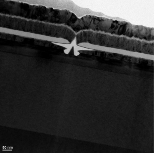
The image above, courtesy of the researchers, shows a cross-section transmission electron micrograph of the fabricated transistor. The central inverted V is the gate. The two molybdenum contacts on either side are the source and drain of the transistor. The channel is the InGaAs light colour layer under the source, drain, and gate.
Although many of the techniques applied by the MIT team are already used in silicon fabrication, they have only rarely been used to make compound semiconductor transistors. This is partly because in applications such as fibre-optic communication, space is less of an issue.
"But when you are talking about integrating billions of tiny transistors onto a chip, then we need to completely reformulate the fabrication technology of compound semiconductor transistors to look much more like that of silicon transistors," del Alamo says.
The team presents its work this week at the International Electron Devices Meeting in San Francisco.
Their next step will be to work on further improving the electrical performance, and hence the speed of the transistor by eliminating unwanted resistance within the device. Once they have achieved this, they will attempt to further shrink the device, with the ultimate aim of reducing the size of their transistor to below 10 nm in gate length.
Matthias Passlack, of Taiwanese semiconductor manufacturer TSMC, says del Alamo's work has been a milestone in semiconductor research. "He and his team have experimentally proven that indium arsenide channels outperform silicon at small-device dimensions," he says. "This pioneering work has stimulated and facilitated the development of CMOS-compatible, III-V-based-technology research and development worldwide."
The research was funded by DARPA and the Semiconductor Research Corporation.


