
Germanium p-Type Transistor Boasts Highest Ever "˜Carrier Mobility'
Almost all computer chips use two types of transistors: p-type (positive), and n-type (negative). Improving the performance of the chip as a whole requires parallel improvements in both types.
At the IEEE's International Electron Devices Meeting (IEDM) in December, researchers from MIT's Microsystems Technology Laboratories (MTL) presented a p-type transistor which they claim has the highest "carrier mobility" yet measured. By that standard, the device is twice as fast as previous experimental p-type transistors and almost four times as fast as the best commercial p-type transistors.
Like other experimental high-performance transistors, the new device derives its speed from its use of a material other than silicon.
The researchers in this case, used germanium. Alloys of germanium are already found in commercial chips, so germanium transistors could be easier to integrate into existing chip-manufacturing processes than transistors made from more exotic materials.
The new transistor also features what's called a trigate design, which could solve some of the problems that plague computer circuits at extremely small sizes (and which Intel has already introduced in its most advanced chip lines). For all these reasons, the new device offers a tantalising path forward for the microchip industry - one that could help sustain the rapid increases in computing power, known as Moore's Law, that consumers have come to expect.
Pluses and minuses
A transistor is a switch that in one position allows charged particles to flow through it ; in the other position, it doesn't. In an n-type transistor, the electrons, which are the charge carriers, produce an ordinary electrical current.
In a p-type transistor, the charge carriers are positively charged "holes." A p-type semiconductor doesn't have enough electrons to balance out the positive charges of its atoms; as electrons hop back and forth between atoms, trying futilely to keep them electrically balanced, holes flow through the semiconductor, in much the way waves propagate across water molecules that locally move back and forth by very small distances.
"Carrier mobility" measures how quickly charge carriers - whether positive or negative - move in the presence of an electric field. Increased mobility can translate into either faster transistor switching speeds, at a fixed voltage, or lower voltage for the same switching speed.
For decades, each logic element in a computer chip has consisted of complementary n-type and p-type transistors whose clever arrangement drastically reduces the chip's power consumption. According to the MIT scientists, in general, it's easier to improve carrier mobility in n-type transistors; the MTL researchers' new device demonstrates that p-type transistors should be able to keep up.
Handling the strain
The researchers from MIT and the University of British Columbia achieved their "record-setting" hole mobility by "straining" the germanium in their transistor. This forced its atoms closer together than they'd ordinarily find comfortable. To do that, they grew the germanium on top of several different layers of silicon and a silicon-germanium composite. The germanium atoms naturally try to line up with the atoms of the layers beneath them, which compresses them together.
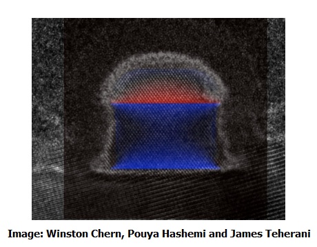
The micrograph at the top of this story, shows an experimental transistor. Blue highlighting indicates areas of "strain," where germanium atoms have been forced closer together than they find comfortable. One of the reasons for the transistor's record-setting performance is that the strain has been relaxed in the lateral direction.
"It's kind of a unique set of material structures that we had to do, and that was actually fabricated here, in the MTL," professor of electrical engineering and computer science at MIT, Hoyt says. "That's what enables us to explore these materials at the limits. You can't buy them at this point."
"These high-strain layers want to break," Teherani, lead author of a paper describing the work, adds. "We're particularly successful at growing these high-strain layers and keeping them strained without defects."
Indeed, Hoyt is one of the pioneers of strained-silicon transistors, a technology found today in almost all commercial computer chips. At last year's IEDM, she and Eugene Fitzgerald, the Flemings-SMA Professor of Materials Science and Engineering at MIT, received the IEEE's Andrew S. Grove Award for outstanding contributions to solid-state devices and technology. The award announcement cited Hoyt's "groundbreaking contributions involving strained-silicon semiconductor materials."
Gatekeeping
Another crucial aspect of the new transistor is its trigate design. If a transistor is a switch, throwing the switch means applying a charge to the transistor's "gate." In a conventional transistor, the gate sits on top of the "channel," through which the charge carriers flow.
As transistors have grown smaller, their gates have shrunk, too. But at smaller sizes, that type of lockstep miniaturisation won't work: Gates will become too small to reliably switch transistors off.
In the trigate design, the channels rise above the surface of the chip, like boxcars sitting in a train yard. To increase its surface area, the gate is wrapped around the channel's three exposed sides - hence the term "trigate." By demonstrating that they can achieve high hole mobility in trigate transistors, Hoyt and her team have also shown that their approach will remain useful in the chips of the future.
"The germanium part helps in increasing the drive current, and the trigate part helps in reducing the leakage in the off state," says Krishna Saraswat, the Rickey/Nielsen Professor in Engineering at Stanford University, who was not involved in this research. "So a combination of those two just gives you an ideal transistor for the next generation."
Saraswat believes that the semiconductor industry is already planning a move toward germanium circuits. "The choice is to scale the silicon transistor without any performance gains - just get to higher packing density - or get higher packing density as well as better performance," he says. "And it's fairly clear that the industry will go for high-strain germanium."
The MIT researchers' work was supported by the U.S. Defence Advanced Research Projects Agency and the Semiconductor Research Corporation.


