
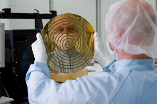
Wafer chucks for 450mm wafer inspection
Berliner Glas, has introduced a series of high precision, custom designed wafer chucks to the semiconductor industry.
Inspection and review systems benefit from very precise adjustment and documentation of flatness and technical advanced materials.
Light and very stiff as well as functional optimised materials based on high performance glasses, glass ceramics and ceramics are ready for 450mm. Special requirements such as high speed rotating and very low run out are maintained by application of these advanced materials.
Thermal influence on the wafer flatness is controlled by using adapted cooling and CTE fitted materials. In combination with new algorithms for designing optimal mesa structures best flatness is adjusted to the requirement of each application.
Very fast chucking and de-chucking times of less than half a second for coulomb type electrostatic chucks as well as vacuum flow optimised chucks increase the wafer throughput and lead to high efficiency for inspection systems.
Hard ceramic coatings minimise adhesion effects of wafers and improve the life time of electrostatic and vacuum chucks. Intelligent electrical controlling drives the chucking and de-chucking response to an optimum b minimizing material specific polarization effects.
Materials are chosen according to their field of application and are designed with regard to temperature requirements, type of radiation and other critical physical aspects. Due to the varying properties of these different materials the chucking performance like clamping pressure and homogeneity is measured and analysed with a special setup using interferometry.
The capability for modelling the effective clamping pressure based on specific material parameters in combination with a high effective three dimensional FE analysis of the electrostatic chuck enables the constant development of new advanced electrostatic chucks.
Berliner Glas will present a broad spectrum of its products and solutions at the Photonics West conference at booth #2228 in San Francisco, California.


