Yole: Manufacturing innovations to propel MEMS equipment market

MEMS packaging is evolving in a different direction to front-end processing. Packaging standardisation will become increasingly critical in order to support the massive volume growth in unit shipments, and decrease overall costs
Though MEMS standardisation will never happen, companies are optimising their own technology platforms.
Such process innovations will drive MEMS equipment and materials to a 7 percent CAGR over 2012-2018.
In its new report "MEMS Front-End Manufacturing Trends", Yole Développement (Yole) goes further in the equipment & materials market forecasts and in the manufacturing trends for MEMS. The report gives detailed analyses about MEMS device technology process flow, manufacturing trends and manufacturing cost breakdown (accelerometers/gyroscopes, microphones, pressure sensors, optical MEMS).
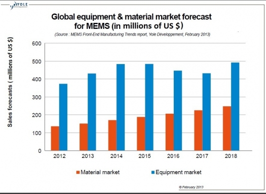
Changes in MEMS manufacturing will drive the equipment & materials market from $378 million to $512 million for equipment and $136 million to $248 million for materials between 2012-2018.
Innovative processes are fuelling the MEMS equipment & materials market. Yole forecasts that demand for MEMS-related equipment will grow from around $378 million in 2012 to over $510 million by 2018, at a CAGR of 5.2 percent over the next five years. It's interesting to note that the MEMS market forecast will follow a cyclical up/downturn similar to what the mainstream IC equipment market underwent.
The demand for materials and related MEMS consumables will grow from about $136 million in 2012 to over $248 million by 2018 at a CAGR of 10.5 percent over the next five years.
As MEMS become commodity products, manufacturing will change and mature.
Today, MEMS fabrication is still very diversified and lacking in standardisation; Yole's rule, "One product, one process" still applies. Indeed, MEMS has taken a different path from ICs and doesn't follow the same roadmap as the semiconductor industry. Thus, it's still common to see many players with radically different manufacturing approaches for the same MEMS device, sometimes within the same company (i.e. both the CMOS MEMS and hybrid approaches can be used for inertial devices or microphones).
However, as MEMS becomes a commodity product with a quicker time-to-market compared to previous generations, anything that speeds up the commercialisation process is welcome. MEMS packaging is evolving in a different direction than front-end processing, and Yole has already identified that packaging standardisation will become increasingly critical in order to support the massive volume growth in unit shipments, and decrease overall costs associated with MEMS & sensor content.
For example, microphone packaging is very similar between one manufacturer and another. What's more, the front-end level, companies are developing in-house technological platforms targeted for different MEMS devices.
Yole believes that as MEMS moves from competing on process technology to competing on functions and systems, a move towards more standard solutions is necessary to drive down package size and cost.
Currently, MEMS foundries still compete at the process level and have to propose a wide range of processes in order to cope with new MEMS designs and structures. This approach differs from fabless companies, which usually focus on one type of MEMS design. Their main objective is to find the most experienced and reliable foundry partner in order to convince customers of their expertise.
IDMs, meanwhile, generally rely on robust and established MEMS processes to manufacture their products.
Foundries, which must always remain at the forefront of changes in the MEMS manufacturing landscape, have the biggest challenge.
TSV & unique wafer stacking solutions are key enablers for reducing die size and cost. What's more, TSV for CSP is gradually seeping into the MEMS industry.
However, since miniaturisation will be limited, new detection principles are currently being developed at various R&D Institutes (i.e. Tronic's M&NEMS concept) in order to lower MEMS size at the silicon level.
This technology is based on piezoresistive nanowires rather than pure capacitive detection, and is poised to be a leap forward in terms of device performance and chip size. This will set the stage for a new generation of combo sensors for Motion Sensing applications, achieving both significant surface reduction and performance improvement for multi-DOF sensors.
Other MEMS technologies, such as gold bonding, could be widely used to reduce die size while maintaining great hermeticity for wafer level packaging.


