
KLA-expands lithography/etch process control family
The firm's new metrology and inspection tools facilitate advanced patterning techniques for manufacturing sub-20nm memory and microprocessor chips
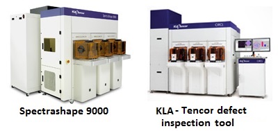
At the SPIE Advanced Lithography conference, KLA-Tencor Corporation revealed its SpectraShape 9000 optical critical dimension (CD) metrology system and BDR300 backside defect inspection and review module.
The SpectraShape 9000 is a new metrology system capable of monitoring the shapes of three-dimensional transistors, memory cells and other key structures that enable high-performance memory and microprocessor chips.
The BDR300 inspects and reviews the back side of the wafer for defects that can cause patterning problems on the wafer's front side. The two new systems are designed to enable volume production of integrated circuits at sub-20nm design rules.
"In this era of highly extended 193nm immersion lithography, our customers are innovating on several fronts to deal with process tolerances in lithography and etch that have become remarkably tight," says Brian Trafas, chief marketing officer at KLA-Tencor.
"The two products we have launched today tackle two key process control issues in this area: scanner focus-related defects and failure or underperformance of finFETs, vertically stacked NANDs, and other three-dimensional structures, caused by small deviations in shape. The BDR300 and SpectraShape 9000 are designed to help our customers navigate the monumental challenges they are facing today in lithography and etch."
The new SpectraShape 9000 introduces a laser-driven plasma light source and several other significant advances that enable leading-edge dimensional metrology capability for a broad range of materials and structures.
The SpectraShape 9000 features higher sensitivity and throughput than its predecessor in order to accommodate the industry's need for tighter process control at sub-20nm nodes - a need to measure more sites per wafer on an increasing number of layers. It also supports innovative metrology targets designed for multiple-patterning lithography.
The new BDR300 back-side inspection and review module for the CIRCL cluster tool features a dramatic improvement in defect sensitivity over that of its predecessor, allowing fabs to find and classify sub-micron back-side defects, which can agglomerate and affect yield at advanced nodes.
The CIRCL cluster is now available as a stand-alone back-side inspection and review system, a configuration designed to support an increasing industry requirement to inspect the back sides of wafers before wafers enter the scanner. Clean wafer back sides reduce the probability of contaminating the scanner chuck and affecting subsequent product.
Multiple SpectraShape 9000 shape metrology systems have been installed at leading logic and memory chip manufacturers, where they are replacing existing CD/shape metrology tools for new technology development and ramp or fulfilling requirements for additional metrology capacity.
The first CIRCL tools containing the BDR300 module have also been installed and are being used for proactive scanner monitoring as well as traditional after-develop defect inspection. To maintain the high performance and productivity demanded by leading-edge production, the SpectraShape and CIRCL tools are backed by KLA-Tencor's global service network.


