Cu pillar and micro-bumping reinvigorate Flip-Chips

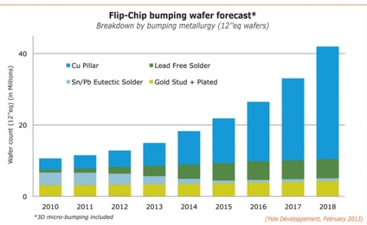
Over the next five years, wafer growth is expected to triple for the Flip-Chip platform, which will reach over 40 million of 12''eq wspy by 2018.
This is according to Yole Développement's "Flip Chip Market and Technology Trends" report, which updates the business status of the Flip-Chip market including data for TIM, underfills, substrates and Flip-Chip bonders.
Despite its high 19 percent CAGR, Flip-chip is not new - in fact, it was first introduced by IBM over 30 years ago. As such, it would be easy to consider it an old, uninteresting, mature technology"¦ but this is far from true. Instead, Flip-Chip is keeping up with the times and developing new bumping solutions to serve the most advanced technologies, like 3DIC and 2.5D.
Indeed, no matter what packaging technology you're using, a bumping step is always required at the end. In 2012, bumping technologies accounted for a massive 81 percent of the total installed capacity in the middle end area. This represents over 14 million 12''eq wafers. What's more, fab loading rates are high, especially for the Cu pillar platform (88 percent).
Flip-Chip is also big on value: in 2012 it was a $20 billion market (making it the biggest market in the middle-end area), and Yole expects it to continue growing at an 9 percent clip, ultimately reaching a whopping $35 billion by 2018.
Flip-Chip capacity is expected to grow over the next five years to meet large demand from three main areas. These are CMOS 28nm IC, including new applications like APE and BB, next generation DDR memory and 3DIC/2.5D interposer using micro-bumping.
Driven by these applications, Cu pillar is on its way to becoming the interconnect of choice for Flip-Chip.
In addition to traditional applications which have used Flip-Chip for a while now (laptop, desktop and their CPUs, GPUs & Chipsets - which are growing slowly but still represent significant production volumes for Flip-Chip), Yole's analyst expects to see strong demand from mobile & wireless (smartphones), consumer applications (tablets, smart TV, set top box), computing and high performance/ industrial applications such as network, servers, data centres and HPC.
The new "Flip-Chip packaged ICs" are expected to radically alter the market landscape with new specific motivations that will drive demand for wafer bumping. "In the context of 3D integration and the "More than Moore" approach, Flip-Chip is one of the key technology bricks and will help enable more sophisticated system on chip integration than ever before," says Lionel Cadix, Market & Technology Analyst, Advanced Packaging, at Yole Développement.
Flip-Chip is being reshaped by a new kind of demand that is hungry for Cu pillars and micro-bumps, which are on their way to becoming the new mainstream bumping metallurgy for die interconnection.
Meanwhile, Cu pillar is fast becoming the interconnect of choice for advanced CMOS (less than 28nm), memory, and micro-bumping for 2.5D interposer and 3DIC.
Yole believes Cu pillar bumping, which is becoming increasingly popular for a wide variety of applications. The massive adoption of Cu pillars is motivated by a combination of several drivers, including very fine pitch, no UBM needed, high Z standoff, etc.
Cu pillar Flip-Chip is expected to grow at a 35 percent CAGR between 2010-2018 in terms of wafer count. Production is already high at Intel, the #1 Flip-Chip producer - and by 2014, more than 50 percent of bumped wafers for Flip-Chip will be equipped with Cu pillars.
As early as 2013, micro-bumping for 2.5D & 3DIC, in conjunction with new applications like APE, DDR memory, etc., will boost Flip-Chip demand and create new challenges and new technological developments (see figure on the left). Today, Flip- Chip is available in a wide range of pitches to answer the specific needs of every application.
The ultimate evolution in bumping technologies will consist of directly bonding IC with copper pads.
3D integration of ICs using this bump-less Cu-Cu bonding is expected to provide an IC-to-IC connection density higher than 4 x 105 cm-2, making it suitable for future wafer-level 3D integration of IC in order to augment Moore's Law scaling.
Taiwan is the #1 location for Flip-Chip bumping according to Yole.
The major OSATs are preparing to produce fcBGA based Cu pillar packages and won't limit the reach of cu pillar bumping to fcCSP. This will allow every company involved in CPU, GPU Chipset, APE, BB, ASIC, FPGA and Memory to access Cu pillar Flip-Chip technology.
Cu pillar capacity is expected to grow rapidly over the 2010 - 2014 timeframe (31 percent CAGR), hitting ~ 9 million wspy by 2014 and supporting the growing demand for micro-bumping and advanced CMOS IC bumping.
In the mutating middle-end area, CMOS foundries now propose wafer bumping services (TSMC, GLOBALFOUNDRIES, etc.), as opposed to bumping houses, which are dedicated to bumping operations (FCI, Nepes, etc.), and OSATs, which keep investing in advanced bumping technologies.
In 2012, OSATs owned 31 percent of installed capacity in ECD solder bumping and 22 percent of installed capacity in Cu pillar bumping. A full overview of 2012 installed capacities for all bumping platforms is provided in this report.
Regionally, Taiwan has the biggest overall bumping capacity (regardless of the metallurgy), with important capacity coming from foundries and OSAT factories. Taiwan currently leads the outsourcing "solder & copper" Flip-Chip wafer bumping market. Flip-Chip market growth, spurred on by the emergence of the "middle-end" environment, has challenged traditional "IDM vs. fabless" supply chain possibilities more than ever before.


