
ST & CMP to support MEMS technology research
A new initiative between the two firms sets to advance new application developments in motion sensing
STMicroelectronics' THELMA MEMS manufacturing process, is now available for prototyping to universities, research labs and design companies through the silicon brokerage services provided by Circuits Multi Projets (CMP).
ST is releasing this process technology to third parties as a prototyping and foundry service. This is to encourage new developments in motion-sensing applications for consumer, automotive, industrial and healthcare markets.
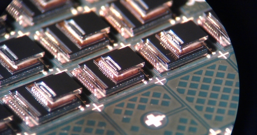
The THELMA MEMS process is used in ST's accelerometers and gyroscopes, which have shipped in billions of units.
ST's long-term success in MEMS (Micro-Electro-Mechanical Systems) sensors has drawn upon its company-developed manufacturing processes. The 0.8µm, surface micro-machining THELMA (Thick Epitaxial Layer for Micro-gyroscopes and Accelerometers) process combines variably thick and thin poly-silicon layers for structures and interconnections.
This enables the integration of linear and angular mechanical elements in a single chip, delivering significant cost and size benefits to customers.
The CMP multi-project wafer service allows organisations to obtain small quantities of advanced ICs manufactured using the same process technologies as would be used on much higher-volume products. Numbers could range from typically a few dozen to a few thousand units.
The THELMA process design rules and design kits are now available for universities and microelectronics companies and the first requests are already being answered.
The introduction of ST's MEMS manufacturing process in CMP's catalogue builds on the successful collaboration that has allowed universities and design firms to access ST's semiconductor manufacturing processes. These range from 130nm CMOS, introduced in 2003, up to the 28nm FD-SOI technology, released for prototyping in late 2012. The initiative will enable the efficient design of next-generation mobile devices that simultaneously require high performance and low power consumption.
"The small-scale availability of our industry-leading MEMS process alongside CMOS technologies including the game-changing FD-SOI, complemented with CMP's advanced service capabilities, offers unprecedented access to state-of-the-art in chip manufacturing for start-ups and R&D labs looking to design intelligent sensor systems," says Benedetto Vigna, Executive Vice President, General Manager, Analogue, MEMS & Sensors Group, STMicroelectronics.
He continues, "With leading-edge industrialised processes at their fingertips, innovators can now concentrate on developing new products rather than investing time and resources in developing technologies."
"Anticipating huge development in MEMS, CMP was the first silicon brokerage service in the world to offer MEMS technologies as early as in 1995," notes Bernard Courtois, Director of CMP.
"Today, CMP is expanding the very successful ST partnership to the THELMA process, offering both the CMOS part and the MEMS part from a single manufacturer. Going beyond inertial sensors, pressure sensors, microphones, e-compasses etc., the ST-CMP partnership will allow CMP customers to move towards complex, embedded systems, addressing more and more societal needs, as components of the Internet of Things," concludes Courtois.


