GLOBALFOUNDRIES develops 3D TSV on 20nm technology

The firm's Fab 8 facility in New York can deliver functional 20nm silicon with Through-Silicon-Vias (TSVs)
GLOBALFOUNDRIES says it has achieved a key milestone in its strategy to enable 3D stacking of chips for next-generation mobile and consumer applications.
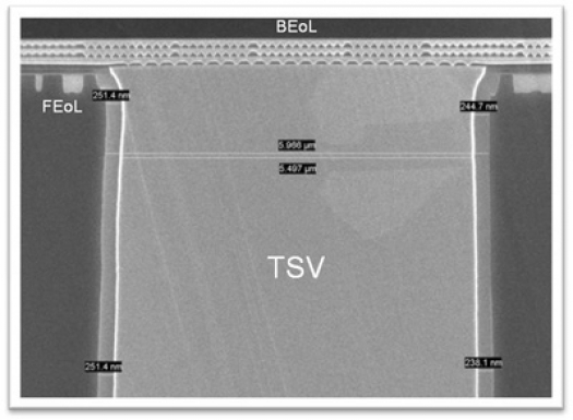
At its Fab 8 campus in Saratoga County, New York, the company has demonstrated its first functional 20nm silicon wafers with integrated Through-Silicon Vias (TSVs).
Manufactured using GLOBALFOUNDRIES' 20nm-LPM process technology, the TSV capabilities will allow customers to stack multiple chips on top of each other, providing another avenue for delivering the demanding performance, power, and bandwidth requirements of today's electronic devices.
TSVs are vertical vias etched in a silicon wafer that are filled with a conducting material, enabling communication between vertically stacked integrated circuits.
The adoption of three-dimensional (3D) chip stacking is increasingly being viewed as an alternative to traditional technology node scaling at the transistor level.
However, TSVs present a number of new challenges to semiconductor manufacturers.
GLOBALFOUNDRIES uses a "via-middle" approach to TSV integration; it inserts the TSVs into the silicon after the wafers have completed the Front End of the Line (FEOL) flow and prior to starting the Back End of the Line (BEOL) process. This approach avoids the high temperatures of the FEOL manufacturing process, allowing the use of copper as the TSV fill material.
To overcome the challenges associated with the migration of TSV technology from 28nm to 20nm, GLOBALFOUNDRIES engineers have developed a proprietary contact protection scheme. This scheme enabled the company to integrate the TSVs with minimal disruption to the 20nm-LPM platform technology, demonstrating SRAM functionality with critical device characteristics in line with those of standard 20nm-LPM silicon.
"Our industry has been talking about the promise of 3D chip stacking for years, but this development is another sign that the promise will soon be a reality," says David McCann, vice president of packaging R&D at GLOBALFOUNDRIES.
"Our next step is to leverage Fab 8's advanced TSV capabilities in conjunction with our OSAT partners to assemble and qualify 3D test vehicles for our open supply chain model, providing customers with the flexibility to choose their preferred back-end supply chain."
As the fabless-foundry business model evolves to address the realities of today's dynamic market, foundries are taking on increasing responsibility for managing the supply chain to deliver end-to-end solutions that meet the requirements of the broad range of leading-edge designs.
To help address these challenges, GLOBALFOUNDRIES is engaging early with partners to jointly develop solutions that will enable the next wave of innovation in the industry. This approach will give customers maximum choice and flexibility, while delivering cost savings, faster time-to-volume, and a reduction in the technical risk associated with developing new technologies.
Indeed, foundries are faring pretty well at the moment. According to a recent report by IC Insights, in 2012, the pure-play foundries and fabless companies were the star performers in the semiconductor industry, demonstrating the most growth.


