
Silicon atoms dance in graphene
Jumping silicon atoms are the stars of an atomic scale ballet featured in a new Nature Communications study from the Department of Energy's Oak Ridge National Laboratory.
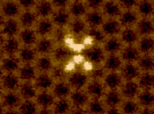
The image above shows a high resolution image supplied by ORNL researchers showing the 'dancing' motions of silicon atoms, pictured in white, in a graphene sheet.
The ORNL research team documented the atoms' behaviour by first trapping clusters of silicon atoms, in a single-atom-thick sheet of carbon known as graphene.
The silicon clusters, composed of six atoms, were pinned in place by pores in the graphene sheet, allowing the team to directly image the material with a scanning transmission electron microscope (or STEM).
The scientists say that the "dancing" movement of the silicon atoms was caused by the energy transferred to the material from the electron beam of the team's microscope.
"It's not the first time people have seen clusters of silicon," says Juan Carlos Idrobo, a co-author of the paper. "The problem is when you put an electron beam on them, you insert energy into the cluster and make the atoms move around. The difference with these results is that the change that we observed was reversible. We were able to see how the silicon cluster changes its structure back and forth by having one of its atoms 'dancing' between two different positions."
Other techniques to study clusters are indirect, points out Jaekwang Lee, first author on the ORNL study. "With the conventional instrumentation used to study clusters, it is not yet possible to directly identify the three-dimensional atomic structure of the cluster," he adds.
The ability to analyse the structure of small clusters is important for scientists because this insight can be used to precisely understand how different atomic configurations control a material's properties. Molecules could then be tailored for specific uses.
"Capturing atomic clusters inside patterned graphene nanopores could potentially lead to practical applications in areas such as electronic and optoelectronic devices, as well as catalysis," Lee continues. "It would be a new approach to tuning electronic and optical properties in materials."
The ORNL team confirmed its experimental findings with theoretical calculations, which helped explain how much energy was required for the silicon atom to switch back and forth between different positions.
The paper is entitled, "Direct visualization of reversible dynamics in a Si6 cluster embedded in a graphene pore," and is available online at the address: http://www.nature.com/ncomms/journal/v4/n4/full/ncomms2671.html.
This research was supported by National Science Foundation, DOE's Office of Science, the McMinn Endowment at Vanderbilt University, and by DOE's Office of Science User Facilities: ORNL's Shared Research Equipment User Facility Program and the National Energy Research Scientific Computing Center at Lawrence Berkeley National Laboratory.


