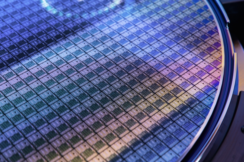
Henkel enables semiconductor package-level EMI shielding
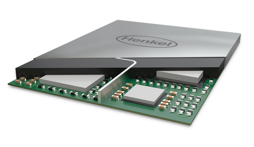
Henkel Adhesive Technologies' Electronics business has announced the introduction of two novel, conformal coating metal inks for semiconductor package-level electromagnetic interference (EMI) shielding.
LOCTITE ABLESTIK EMI 8660S and LOCTITE ABLESTIK EMI 8880S offer superior flexibility in deployment and design, as they may be used with cost-effective spray coating equipment, while providing EMI shielding performance comparable to or better than capital-intensive, thin film metal deposition techniques. With excellent adhesion to a variety of epoxy molding compounds, both materials enhance long-term reliability performance. "The proliferation of higher-frequency wireless communication standards, the continuing expansion of device functionality alongside decreasing component size, and the increase in printed circuit board (PCB) densities have accelerated the need for more effective and adaptable package-level EMI shielding solutions," explains Jinu Choi, Henkel Market Segment Head for Emerging Applications in Semiconductor Packaging Materials.
"Henkel's new conformal shielding inks enable the deposition of an ultra-thin, highly electrically conductive layer that provides the shielding effectiveness of pure metal, with greater production scalability at a fraction of the cost of other shielding methods. Our solutions are distinctive, providing shielding effectiveness up to 80 percent higher than traditional organic-based conductive inks."
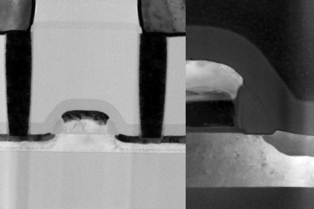
Because the materials can be used with market-available spraying methods, they address the high capital costs, throughput limitations and process complexities associated with physical vapor deposition and plating. Using commercially-available, fine-mist technologies like ultrasonic spraying, the inks are applied directly onto the surface of a molded component with top and sidewall coverage uniformity. The solution allows for simplified, automated, multi-part processing for reduced cost and increased units per hour (UPH) as compared to alternative techniques.
LOCTITE ABLESTIK EMI 8660S provides shielding at a frequency range of 500 MHz to 10 GHz, while LOCTITE ABLESTIK EMI 8880S offers effective shielding for a wider range of 10 MHz to 10 GHz. The thermally-cured coatings may be deposited as thin as 3 to 5 μm to accommodate slim, next-generation package profiles, and are compatible with Henkel compartment shielding materials used to isolate components within System-in-Package (SiP) devices. LOCTITE ABLESTIK EMI 8880S and LOCTITE ABLESTIK EMI 8660S conformal coating metal inks are available for immediate sampling.
The new EMI shielding solutions will be presented on September 14, 2017 at 11:00 a.m. in Henkel hospitality suite #403 at Semicon Taiwan, held at the Taipei Nangang Exhibition Center. Space is limited and allocated on first-come, first-served basis.