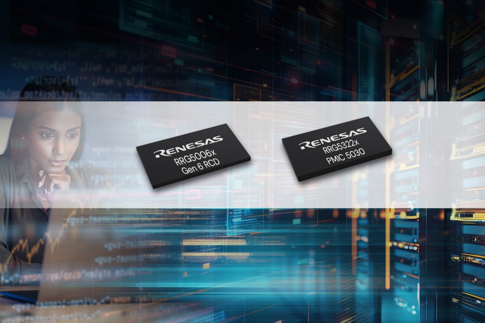
ACM Research delivers first Horizontal Panel Electroplating Tool
ACM’s Ultra ECP ap-p enables next generation device performance amid accelerating market demand for advanced packaging.
ACM Research has delivered the first panel electrochemical plating tool, the Ultra ECP ap-p, to an industry-leading panel fabrication customer. This achievement underscores ACM’s advancement in panel-level electroplating technology and reflects growing market demand for scalable, cost-efficient advanced packaging solutions to meet next generation device requirements.
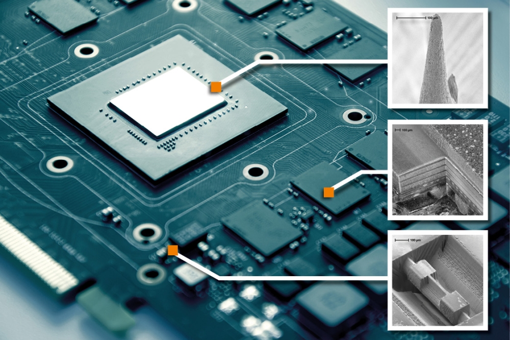
The Ultra ECP ap-p is the first commercial panel-level copper deposition system for the large-panel market, supporting plating steps across pillar, bump, and redistribution layer (RDL) processes. The system achieves panel-processing performance - comparable to traditional round wafer processes, enabling manufacturers to meet demanding device requirements with greater efficiency.
“We are pleased to fulfill this order for our Ultra ECP ap-p,” said Dr. David Wang, ACM’s President and Chief Executive Officer. “This milestone demonstrates our ability to deliver high-performance horizontal panel electroplating solutions through our differentiated technology that help customers accelerate their fan-out panel-level packaging roadmaps while strengthening our role in the advanced packaging ecosystem. As demand grows for next-generation devices, panel-level packaging offers the scalability, throughput, and cost advantages needed for high-volume production, which will achieve a seamless transition for the industry from 300-millimeter wafer packaging to panel-level packaging.”
The system features ACM proprietary horizontal electroplating technology, and supports copper (Cu), nickel (Ni), tin-silver (SnAg) and a gold (Au) plating. The Cu plating chambers incorporate high-speed plating paddles specifically designed for tall pillar applications, capable of achieving pillar heights exceeding 300 microns. The Ultra ECP ap-p features a four-sided sealing dry contact chuck for improved reliability, in-cell rinse functionality to minimize chemical cross-contamination between different plating cells, and a horizontal electroplating design synchronizing a rotating square electrical field with the rotating chuck for superior deposition uniformity.