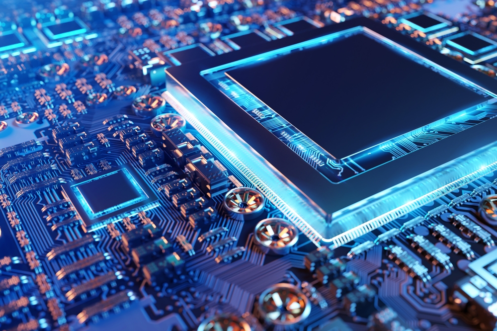
Advanced packaging with glass instead of silicon

TRUMPF and SCHMID Group enable cost-effective high-speed chips.
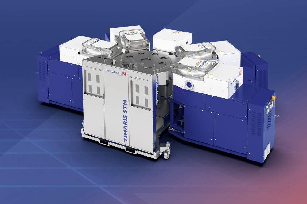
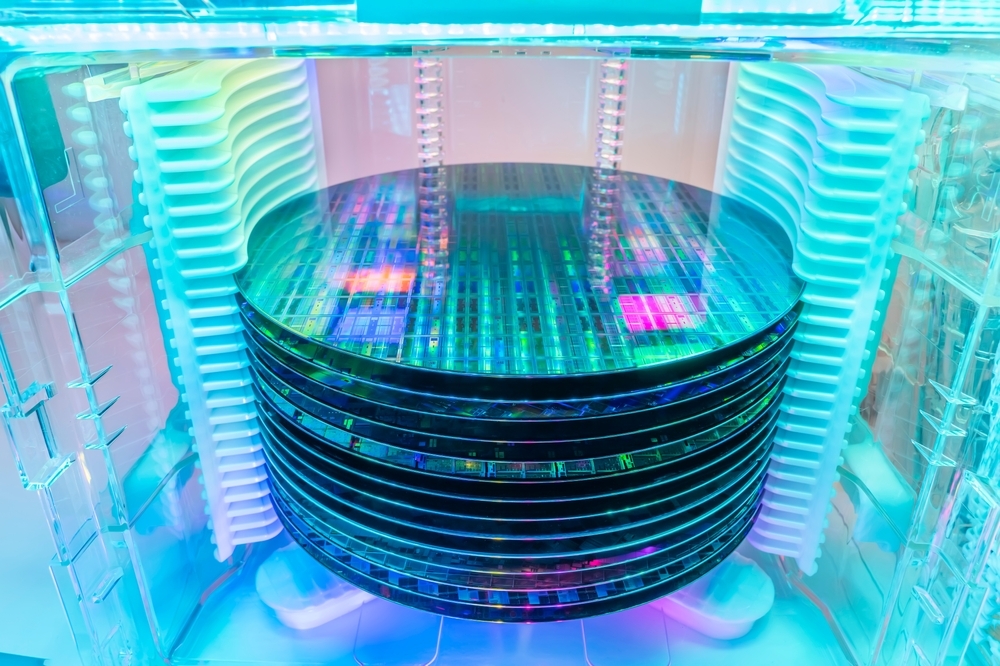
TRUMPF and the SCHMID Group are developing an innovative manufacturing process for the latest microchip generation for the global chip industry. This will enable manufacturers to increase the performance of high-end electronic components for smartphones, smart watches and AI applications. In the process known as advanced packaging, manufacturers combine individual chips on silicon components known as interposers. With the process from TRUMPF and SCHMID, these interposers can be made of glass in the future.
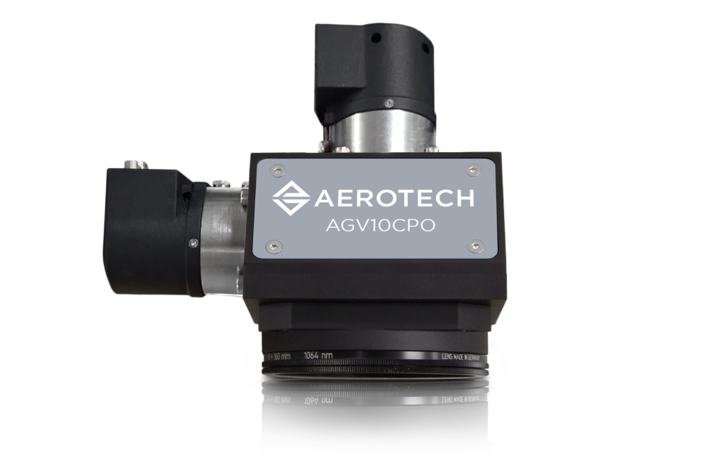
“Advanced packaging with glass is a crucial future technology for the semiconductor industry. Glass is significantly cheaper than silicon. This will enable manufacturers to reduce production costs and make high-performance end devices much more affordable for customers,” says TRUMPF Business Development Manager Christian Weddeling, who is responsible for semiconductors. TRUMPF and SCHMID are developing a combined laser-etching process for advanced packaging with glass. The two companies use a special approach to wet chemistry that shortens process times by a factor of ten. “For this to work well, the laser and wet chemistry must be very well coordinated,” says Weddeling.
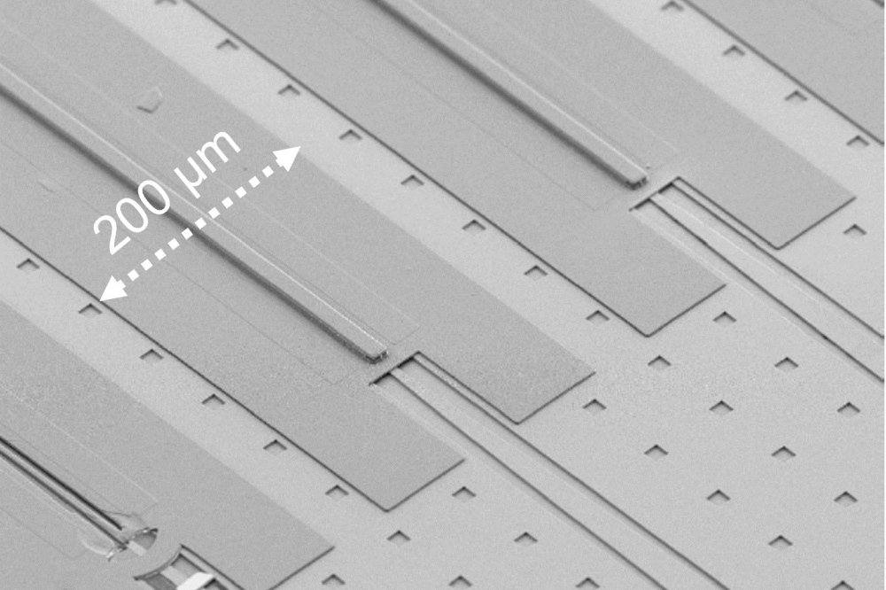
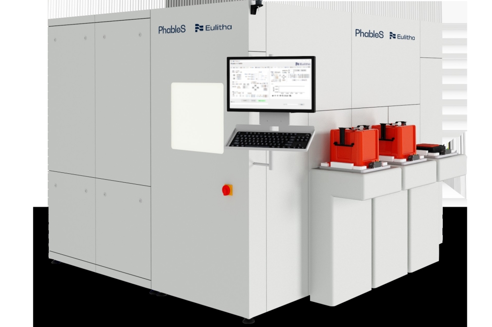
The manufacturing process requires extreme care and precision. This is because the glass used is only between 100 micrometers and one millimeter thin. For comparison, 100 micrometers is about the thickness of a sheet of paper, and one millimeter is about the thickness of a credit card. To create connections on the interposer, manufacturers have to drill holes through the glass, so-called through-glass vias (TGV). Manufacturers often have to create millions of holes in a panel to make the desired connections.
“It is the combination of TRUMPF's laser technology and the SCHMID Group's expertise in etching processes for microchip production that enables efficient production,” says Christian Buchner, responsible for the photovoltaic division at the SCHMID Group. An ultrashort pulse laser from TRUMPF selectively changes the structure of the glass, which is then treated with an etching solution. The desired holes are created at the specified locations and then filled with copper to form the conductor tracks. “The laser and etching processes must be perfectly coordinated to create precise holes. Only through close cooperation between the two companies can we achieve the extreme levels of accuracy that are standard in the industry,” says Buchner.
According to the Boston Consulting Group, the market for advanced microchip packaging is expected to grow to more than 96 billion dollars by 2030. For the high-tech company TRUMPF and the SCHMID Group, a renowned partner of the chip industry, advanced packaging with the help of glass could also develop into an important future market. Currently, applications in consumer electronics such as smartphones dominate the advanced packaging sector. In the future, applications in the field of artificial intelligence are likely to be the growth drivers.