Keysight expands chiplet interconnect standards support

Introduces support for the latest interconnect standards, including Universal Chiplet Interconnect Express™ (UCIe™) 2.0 and Open Compute Project Bunch of Wires (BoW).
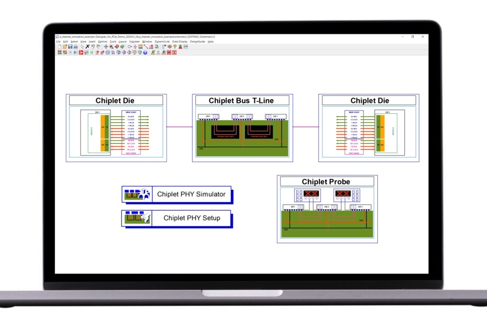
Keysight Technologies has launched Chiplet PHY Designer 2025, its latest solution for high-speed digital chiplet design tailored to AI and data center applications. The enhanced software introduces simulation capabilities for the Universal Chiplet Interconnect Express™ (UCIe™) 2.0 standard and adds support for the Open Computer Project Bunch of Wires (BoW) standard. As an advanced, system-level chiplet design and die-to-die (D2D) design solution, Chiplet PHY Designer enables pre-silicon level validation, streamlining the path to tapeout.
As AI and data center chips grow more complex, ensuring reliable communication between chiplets becomes crucial for performance. The industry is addressing this challenge through open, emerging standards like UCIe and BoW that define the interconnects between chiplets within an advanced 2.5D/3D or laminate/advanced package. By adopting these standards and verifying chiplets for compliance, designers contribute to the growing ecosystem for chiplet interoperability, reducing costs and risks in semiconductor development.
Key Benefits of the Chiplet PHY Designer 2025:
Ensures Interoperability: Verifies designs meet UCIe 2.0 and BoW standards, enabling seamless integration across advanced packaging ecosystems.
Accelerates Time-to-Market: Automates simulation and compliance testing setup, such as Voltage Transfer Function (VTF), simplifying chiplet design workflows.
Improves Design Accuracy: Provides insight into signal integrity, bit error rate (BER), and crosstalk analysis, reducing risks of costly silicon re-spins.
Optimizes Clocking Designs: Supports advanced clocking scheme analysis, such as quarter-rate data rate (QDR), for precise synchronization in high-speed interconnects.
Hee-Soo Lee, High-Speed Digital Segment Lead, Keysight EDA, said: “Keysight EDA launched Chiplet PHY Designer one year ago as the industry’s first pre-silicon validation tool to provide in-depth modeling and simulation capabilities; this enabled chiplet designers to rapidly and accurately verify that their designs meet specifications before tapeout. The latest release keeps pace with evolving standards like UCIe 2.0 and BoW while delivering new features, such as the QDR clocking scheme and systematic crosstalk analysis for single-ended buses. Engineers using Chiplet PHY Designer save time and avoid costly rework, ensuring their designs meet performance requirements before manufacturing. Early adopters, like Alphawave Semi, attest that Chiplet PHY Designer ensures seamless operation and interoperability for 2.5D/3D solutions available to their chiplet customers.”