Indian first for KASFAB Tools

KASFAB Tools has launched India's first manufacturing and building facility dedicated to building semiconductor equipment for global customers.
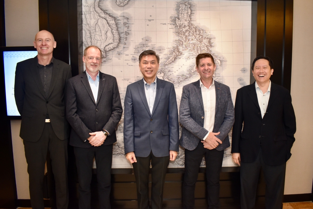
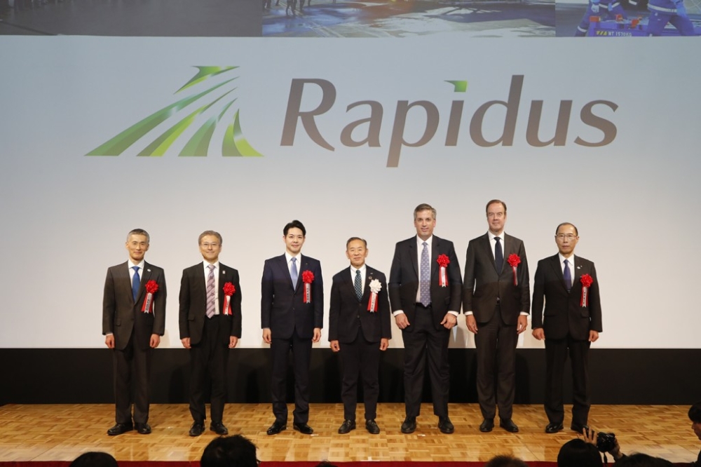
The state-of-the-art facility, located in Doddaballapur, was inaugurated among global supply chain partners and customers from Fortune 100 companies in attendance with Dr. Suraj Rengarajan - Head Semiconductor Products Group in Applied Materials India, Dr. Ankineedu Velaga - SVP & Country Head YES India and Prof. Srinivasan Raghavan - Chairman CeNSe IISc formally inaugurating the facility.
KAS Group, a prominent player with a proven track record in the engineering sector and an impressive portfolio of companies including UHP Technologies and KASTech Equipments serving Solar and Semiconductor Industry with established expertise across multiple domains, such as solar fabs and semiconductor R&D facilities, UHP Technologies has recently been awarded a significant contract for Micron Semiconductor Gujarat, further solidifying its position in the industry.
This groundbreaking initiative marks a significant milestone in India's journey towards self-reliance and leadership in the semiconductor industry. The KAS Group will invest significantly in KASFAB Tools Private Limited, the newly formed company, beginning with INR 20 crore in its initial phase, followed by an additional INR 250 crore in the subsequent expansion phase. This strategic move aims to tap into a global market valued at USD 25 billion, with the Indian semiconductor ecosystem poised to reach INR 2500 crore within the next 3 to 5 years. Projections for FY 2025-26 forecast INR 50 crore in revenue, with expectations for exponential growth in the coming years as the company continues to scale.
"This world-class facility represents a pivotal step in strengthening India's semiconductor ecosystem," said Mr. Manjunath Jyothinagara, Managing Director, KASFAB Tools Pvt. Ltd. "By providing advanced manufacturing capabilities, we are not only supporting global customers but also positioning Karnataka as a leading hub for innovation and high-tech engineering. This initiative will generate employment, attract significant investments, and accelerate India's ambitions to become a global leader in semiconductor manufacturing."
"With first-of-its-kind infrastructure in India, capable of supporting industry giants we look forward to collaborate with players like Applied Materials, LAM Research, Tokyo Electron, Yield Engineering Systems and likes of them. As global semiconductor equipment makers look to diversify their supply chains, India offers a compelling opportunity for contract manufacturing. The country's talent pool and engineering ecosystem will drive MSMEs to embrace this path with greater confidence, and we anticipate a growing number of players will be motivated to join in building a vibrant, local semiconductor ecosystem."
The facility also houses independent test and validation tools, a safety simulation bench, and functional testing capabilities, ensuring compliance with the highest global standards. The facility sprawled across 20,000 sq. ft. on the outskirts of Bangalore, has been developed after extensive benchmarking of similar setups in the USA, Japan, South Korea, Malaysia, and China, making it one of the most advanced facilities of its kind in India.
The new facility is designed to cater to the demands of leading global customers, including Applied Materials, LAM Research, Tokyo Electron and Yield Engineering Systems, among others. It is equipped with cutting-edge infrastructure, including Class 10 and Class 100 cleanrooms, high-precision welding for plastics and metals, component fabrication, and ultrasound-aided cleaning with deionized (DI) water.
The facility is open to showcase its pioneering capabilities including Class 10/Class 100 cleanrooms, precision welding, and comprehensive testing and validation setups.