Innovations focus on photonics and FAMES success
CEA-Leti has been busy in recent weeks, presenting new research at the recent SPIE Photonics West and ISSCC events, as well as focusing on the FAMES pilot line
CEA-Leti presented new research at SPIE Photonics West highlighting major progress in the integration of quantum cascade lasers (QCLs) with silicon photonic platforms for mid-infrared (MIR) applications.
The paper, “Advanced Architectures for Hybrid III-V/Silicon Quantum Cascade Lasers: Toward Integrated Mid-Infrared Photonic Platforms,” compares three complementary hybrid laser architectures that collectively advance the practicality, flexibility, and scalability of MIR photonics.

III-V/Si Distributed FeedBack QCL. Photo credit: Maxime LEPAGE
Toward ‘smaller, more robust, and more manufacturable MIR systems’
Mid-infrared light plays a critical role in technologies such as gas sensing, chemical spectroscopy, biomedical diagnostics, and security, because many molecules exhibit strong absorption signatures in this spectral region. Despite the technology’s importance, MIR photonic systems remain large, costly, and difficult to manufacture at scale. Integrating MIR light sources directly onto silicon photonic platforms offers a path toward smaller, more robust, and more manufacturable systems—bringing mid-infrared photonics closer to the level of integration in the near-infrared.
Three architectures, three integration strategies
In its Photonics West presentation, CEA-Leti demonstrated and compared three distinct hybrid III-V/silicon QCL architectures, each addressing a different integration challenge:
Hybrid distributed feedback QCL on silicon-on-nothing-on-insulator with adiabatic coupling
- This approach enables robust single-mode emission around 4.3 µm with efficient optical power transfer from the III-V active region into silicon waveguides. High-index-contrast silicon photonics provide precise feedback and light routing, making this architecture well suited for scalable photonic integrated circuits targeting spectroscopy and chemical sensing.
Hybrid QCL with an external silicon distributed bragg reflector cavity
- In this configuration, optical gain and optical feedback are decoupled: the III-V material provides amplification, while wavelength selection and feedback are implemented in silicon using distributed Bragg reflector (DBR) cavities. This separation offers enhanced design flexibility and opens a clear path toward tunable and multifunctional MIR sources for advanced spectroscopic and sensing systems.
Ultra-compact QCL micro-sources based on photonic crystals & micro-rings
- Miniature light sources in these devices achieve footprints below 100 µm² by leveraging strong optical confinement and resonant effects. The resulting extreme miniaturization enables dense on-chip integration and supports new system architectures where size, power consumption, and integration density are critical.

III-V/Si Photonic Crystal Surface Emitting QCL & Micro-resonator Ring. Image Credit: Alexis Holb
From passive platform to active host
Collectively, the results show that silicon photonics can play an active role in mid-infrared laser systems. By combining adiabatic optical coupling, silicon-based feedback and cavity engineering, and ultra-compact laser concepts, CEA-Leti establishes several viable integration pathways rather than a single, one-size-fits-all solution. The work highlights how different architectures trade off stability, flexibility, and footprint, providing designers with a practical toolkit for MIR photonic systems.
“By combining quantum cascade lasers with silicon photonics, we are bringing mid-infrared sources closer to the level of integration and scalability that silicon platforms have already achieved in the near-infrared,” said Alexis Hobl, presenter and lead author of the paper.
Looking ahead
Future work will focus on further improving optical coupling efficiency, fabrication robustness, and thermal and electrical management, as well as integrating additional on-chip photonic functions such as filters, multiplexers, and interferometric circuits. Demonstrating wafer-scale reproducibility and packaging-ready designs will be key milestones on the path toward fully integrated mid-infrared photonic systems. Acknowledgements: L’Institut des Nanotechnologies de Lyon (INL), III-V Lab, and Fraunhofer Applied Solid State Physics IAF contributed to this project.
Combined MicroLED and organic photodetector architecture
CEA-Leti also demonstrated a co-packaged microLED and organic photodetector (OPD) architecture that enables optical sensing functions. This solution paves the way to integrate sensing capabilities directly within a microLED display, without compromising display performance. The work, presented in the Photonics West paper, “Co-Packaging of Organic Photodetector with MicroLED Matrix for Multifunctional Display Bio-Application”, validates a system-level approach combining device design, electronics, and modeling for multifunctional display applications.
MicroLEDs deliver high radiance using only a limited fraction of the pixel surface, leaving space for additional functionality. Leveraging this characteristic, CEA-Leti developed a microLED array co-packaged with a tailored OPD, with both devices optimized for operation at green wavelengths relevant to photoplethysmography (PPG) signal extraction.
Technology performance assessment
To move beyond component-level demonstrations, the researchers designed a dedicated electronic platform enabling full end-to-end characterization of the complete signal chain—from microLED driving, through a device under test, to photodetection and readout circuitry. Lock-in detection techniques were implemented to improve signal-to-noise ratio and suppress static parasitic components. This is particularly relevant for biosensing detection where AC/DC ratio should be enhanced.

Illustration of co-packaged OPD and MicroLED matrix. Photo credit: Eric Kroemer/CEA-Leti
System validation was performed using optical phantoms engineered to replicate the absorption and scattering properties of biological tissue. This approach provided a controlled and repeatable environment for assessing biosensing performance under realistic conditions. Experimental results were combined with analytical modeling to derive a closed-form expression linking microLED operating conditions, photodetector responsivity, and device-under-test reflectance to the detected signal.
The co-packaged microLED devices demonstrated optical power up to 12 mW at a wavelength of 525 nm. On the detection side, OPD responsivity was tuned by adjusting the thickness of the ZnPc active layer to align with the microLED emission peak, achieving a responsivity of 0.083 A/W at the wavelength of interest.
Benefits of MicroLED technology
The results show that microLED displays can support integrated optical sensing at the pixel level without forcing trade-offs between brightness, resolution, and sensing area. Unlike OLED-based approaches, where display and sensing functions compete for the same surface, this architecture allows both functions to coexist within the same front plane.

Characterization platform including custom electronic board and biological phantom mimicking human tissues. Photos credit: Eric Kroemer/CEA-Leti
The fully characterized, end-to-end system establishes a technical foundation for displays that combine visual output with integrated sensing and adaptive functions, with potential relevance for next-generation displays. Rather than relying on sensors located usually in the bezel of the display, this approach enables sensing capabilities to be designed directly into the display and widespread.
System-technology co-design approach
“This work illustrates CEA-Leti’s system-technology co-design approach, from concept definition and microLED technology to photodetector co-design, electronics development, and experimental validation under realistic conditions,” said Michaël Pelissier, lead author of the paper. “By combining hardware development with analytical modeling and simulation, we establish a concrete framework for evaluating and scaling sensing-integrated display architectures.”
The study establishes practical know-how for co-integrating microLED displays and optical sensing functions. The architecture is inherently scalable and can be adapted to different pixel pitches and resolutions, depending on the targeted application—from medium-size displays such as smartphones and wearables to larger formats including monitors and televisions.
The results provide a technical foundation for future multifunctional displays in which visual output and sensing capabilities are designed together, at the system level, rather than added as separate components. This work is part of the IPCEI Microelectronics and Connectivity and was supported by the French Public Authorities within the frame of France
2030.
First dynamically routed electro-optical router for photonic interposers
Researchers from CEA-List and CEA-Leti unveiled at ISSCC the first electro-optical router with dynamic, frame-level optical routing integrated with CMOS control logic, marking a major step toward practical optical networking inside advanced chiplet-based packages.

Detail view of the system-on-interposer, with a companion electro-optical router for each computing die and two additional routers for primary IO. Light coupling to the optical network on interposer is achieved on fiber coupling visible on the bottom-right corner. Photo credit: KAM Productions
Their paper, “A 3.19pJ/bit Electro-Optical Router with 18ns Setup Frame-Level Routing and 1-6 Wavelength Flexible Link Capacity for Photonic Interposers”, demonstrates an electro-optical router implemented in 28 nm CMOS on a photonic interposer, capable of establishing optical paths in 18 nanoseconds. It dynamically selects one-to-six wavelengths per link, and achieves an energy efficiency of 3.19 pJ/bit with an active area of just 0.007 mm² per link.
Moving optical links beyond static point-to-point
Today’s optical interconnects are largely limited to static, point-to-point links, with initialization and training times ranging from microseconds to milliseconds. While suitable for board-level or rack-scale communication, those latencies prevent optical links from being used as a true networking fabric inside multi-die packages.
The router addresses this gap by integrating optical switching, routing control, serializer/deserializer (SerDes), and clocking logic directly with silicon photonics. The result is a dynamically routed optical interconnect that operates at nanosecond timescales, enabling optical communication across centimeter-scale interposers with responsiveness previously limited to short electrical links.
It supports frame-level routing, allowing optical paths to be established and torn down on demand, and adjusts link capacity dynamically by selecting between one and six wavelengths, according to application needs. This flexibility enables efficient use of optical bandwidth, while maintaining
ultra-low latency.
Architecture and implementation
The prototype is fabricated in a 28 nm CMOS process and integrated on a photonic interposer. Compact analog drivers, combined with standard-cell-based SerDes and clocking circuits, enable dense integration of optical endpoints close to compute and memory resources. While the architectural target includes CPUs, GPUs, and high-bandwidth memory (HBM) in large 2.5D and 3D packages, the current chip serves as a proof of concept, demonstrated on a small-scale multi-die system derived from CEA-Leti’s earlier INTACT active interposer architecture (ISSCC 2020).
A first integrated dynamic optical routing
This is the first demonstration of dynamic optical routing in an integrated photonic switch that includes CMOS logic up to the protocol level. Previous optical switch demonstrations typically rely on standalone photonic devices with static or slowly reconfigured paths and do not integrate the full driving, control, and routing logic required for packet-level operation.
In contrast, the router operates as a miniature network switch inside the package, combining microring-based photonic devices with digital control logic to move data efficiently across the interposer. Compared with electrical routing fabrics or active interposers, the approach avoids power and latency penalties that scale with distance, relaxing constraints on data locality and enabling more flexible hardware architectures and software data placement.
Enabling new chiplet architectures
By bringing dynamic, ultra-low-latency optical networking into the package, the technology opens new possibilities for high-performance computing, AI accelerators, and data-intensive systems, where growing model sizes and memory demands increasingly stress conventional interconnects.
Rather than forcing all data to reside near compute cores to minimize electrical routing costs, dynamically routed optical links allow architects to treat memory and compute resources across the interposer as part of a unified, high-reach fabric without sacrificing latency or energy efficiency.
“As chiplet systems continue to grow in scale and complexity, the ability to move data efficiently across the entire package becomes essential,” said CEA-List’s Yvain Thonnart, lead author of the paper. “Our goal was to demonstrate that photonic links can provide that reach without sacrificing the flexibility designers expect from modern interconnects. This router is a step toward practical, dynamically routed optical networks that fit within standard CMOS design flows and real product constraints.”
Validating first ultra-fast, battery-operated EPR Spectrometer at chip scale
Researchers at CEA-Leti and CEA-IRIG-SyMMES have validated a chip-scale electron paramagnetic resonance (EPR) spectrometer that achieves unprecedented scan speed, spectral span, and sensitivity from a battery-operated integrated circuit. By replacing the bulky electromagnets used in conventional EPR instruments with an ultra-fast frequency-scanned architecture, the system enables high-performance paramagnetic sensing in portable and space-constrained environments where traditional systems cannot operate.

On-chip EPR spectrometer, fabricated on CMOS GF22nmFDSOI technology. The 4.4mm2 passivated circuit is mounted on a Printed Circuit Board (PCB), and bondings are molded. The sample to be analyzed is directly deposited onto the chip. Photo credit: JB.David_CEA
The results were presented at ISSCC 2026 in the paper “A 1400 THz/s Ultra-Fast-Scan 14 GHz EPR-on-a-Chip Based on Injection-Locked Phase Detection Featuring 120 µM Concentration Sensitivity.”
Miniaturized EPR spectrometers transform a complex laboratory instrument into a portable, low-power microchip capable of detecting reactive chemical species that influence energy storage, materials reliability, environmental safety, and biomedical processes. By eliminating the bulky electromagnet that traditionally limits EPR instruments to centralized facilities, this technology, sometimes dubbed “EPR-on-a-chip”, makes it possible to perform high-precision analysis directly in the field, at industrial sites, or inside research systems where traditional tools don’t fit.
Record performance at milliwatt power levels
The system delivers:
- 1,400 THz/s scan rate
- 100-Gauss equivalent spectral span
- 120 µM concentration sensitivity
- 96 mW power consumption
- 200 ns scan time across the full span
This performance exceeds that of state-of-the-art miniaturized EPR devices, which typically trade sensitivity and spectral range for speed. The combination of ultra-fast scans and wide spectral coverage enables observation of fast-passage effects and transient phenomena in chemical reactions that are difficult or impossible to capture with existing systems.

The 96mW on-chip EPR spectrometer is programmed, driven, and monitored through a dedicated Printed Circuit Board. The PCB aspect-ratio fits with the need to insert the chip inside a 0.5T permanent magnet. Photo credit: JB.David_CEA
New applications across healthcare, materials, and the environment
By shrinking EPR to chip scale, CEA-Leti and CEA-IRIG open new application paths in healthcare diagnostics, materials characterization, and environmental monitoring. Portable, low-power EPR sensing could support on-site chemical analysis, embedded monitoring in research systems, and distributed sensing networks. As development advances toward a full prototype, the technology represents a significant step toward making high-precision spectrometry more accessible and deployable beyond the laboratory.
Injection-locked phase detection enables high sensitivity
At the core of the system is an original injection-locked phase-detection architecture that encodes the EPR signal as a phase shift rather than an amplitude or frequency change. By exploiting the intrinsically low phase noise of injection-locked oscillators, the design achieves unprecedented sensitivity for a single-sensor, chip-scale EPR system.
“Our goal is to create a compact, portable EPR spectrometer that operates on just a few watts of power, enabling on-site analysis in environments where conventional instruments simply cannot operate,” said Serge Gambarelli, research director at CEA-IRIG and EPR spectroscopy expert.
“By adapting RF and frequency-synthesis architectures originally developed for telecommunications, we were able to integrate a complete EPR system on a single 22 nm chip,” said Alexandre Siligaris, senior research engineer at CEA-Leti.
A milestone for european scientific instrumentation
The circuit is the first scientific instrument fabricated using the advanced 22 nm FDSOI technology. While manufactured by GlobalFoundries, an international fab partner of CEA, the system architecture, circuit design, and measurement approach were fully developed and patented by CEA. The work marks a major milestone in CEA’s Moonshot µ-RPE program, which aims to develop a compact, deployable EPR spectrometer to support key missions of CEA—and highlights Europe’s leadership in advanced microelectronics for scientific instrumentation. The Moonshot program also includes R&D on planar magnets, which are key to future spectrometers, because they increase the number and field of applications.
“Typically applied in electric mobility and energy transition sectors, this expertise is now being leveraged to design the magnetic system for the µ-EPR spectrometer, demonstrating a valuable transfer of knowledge into the field of instrumentation,” said Celine Delafosse, laboratory manager at CEA-Liten, which is leading that research area.
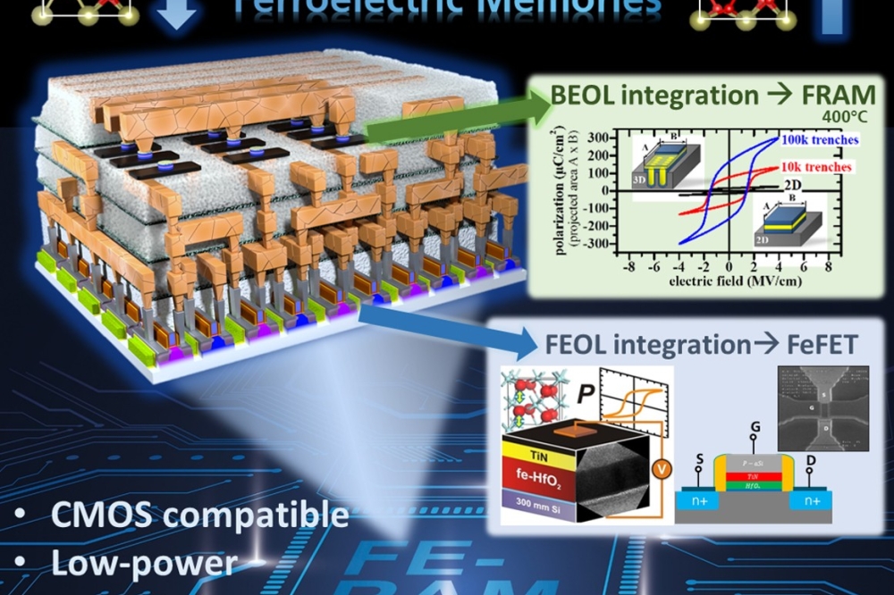
FAMES pilot line inaugurated after delivering
The FAMES Pilot Line was officially inaugurated at the end of January - two years after it began, now delivering validated technical results across advanced FD-SOI, RF, embedded non-volatile memories, 3D integration technologies, and Power Management ICs. Those results, produced on a 300 mm line and reported at leading international conferences, confirm that the European tech-sovereignty initiative is already operating as a working European semiconductor capability.
The inauguration, attended by more than 350 people, marked the launch of a cleanroom extension at CEA-Leti’s Grenoble site. The open-access feature of the pilot line makes the FAMES technologies accessible primarily, but not exclusively, to European startups, SMEs, industrial groups, and research organizations seeking to prototype, qualify, and de-risk advanced semiconductor technologies before industrial deployment. The initiative is coordinated by the CEA.
Technological momentum
Since entering operation, the pilot line has generated concrete advances across its core domains, spanning substrates, embedded ferroelectric non-volatile memories, advanced FD-SOI, 3D integration, high performance RF passive components—areas critical to next-generation chips.
“The breakthrough technologies developed within FAMES are intended to support future generations of sub-10 nm FD-SOI chips, enabling high-performance and low-power components for Europe,” said Jean-René Lèquepeys, deputy director and CTO of CEA-Leti. “Scaling down the FD-SOI technology to 10 and 7nm will bring significant chip performance improvements compared to current nodes, in density, power consumption, speed and radio-frequency behavior.”
Among the most recent milestones, CEA-Leti recently presented results at IEDM 2025 demonstrating fully functional 2.5 V SOI CMOS devices fabricated at a thermal budget of 400 °C. Achieving performance comparable to conventional high-temperature CMOS, the work removes a key barrier to large-scale 3D sequential integration and enables dense multi-tier chip architectures compatible with advanced back-end processes—one of the central technical objectives of FAMES.
Ultra-efficient ecological systems
With 2,000 m² of cleanroom space, the new facility expands CEA-Leti’s cleanroom space to 14,000 m². It will house more than 80 state-of-the-art 300mm cleanroom tools. Two basement levels help manage complex technical installations, and a five-meter ceiling height accommodates large equipment. In addition, very low vibration levels and dedicated electrical back-up systems will ensure uninterrupted operation.
In addition to housing some of the semiconductor industry’s most specialized and sophisticated tools, the facility has been equipped with systems and processes enabling advanced optimization of its environmental footprint. The building incorporates high-performance insulation requirements and will enable the implementation of waste-energy recovery solutions (residual heat recovery).
Following the French France 2030 NextGen project, which was launched in 2022, the FAMES pilot Line project provided additional momentum in 2023 under the EU Chips Act. These two initiatives were designed to shorten the path from research to industrial readiness by providing a leading edge, open-access environment for technology innovation.
‘The role FAMES is meant to play’
“The fact that results are already being published and validated internationally underscores the role FAMES is meant to play,” said Dominique Noguet, vice president at CEA-Leti and coordinator of the pilot line. “This is not a future manufacturing line. It is an operational platform where advanced technologies are being matured, demonstrated, and prepared for transfer to industry.”
With a total investment of €830 million, co-funded by the European Commission under the Chips Act and by participating Member States, FAMES brings together 11 partners across eight countries. Its objective is to reduce the time between research and industrialization, while strengthening Europe’s technological autonomy in semiconductor domains that underpin strategic sectors including automotive, telecommunications, edge AI, industrial systems, health, space, and cybersecurity.
By inaugurating a pilot line that is already producing validated results, FAMES exemplifies the lab-to-industry model at the core of Europe’s semiconductor strategy—providing industry with access to mature technologies, proven processes, and a direct path toward future manufacturing.
‘Fully aligned with the ambition of the chips act’
“With the inauguration of FAMES, the CEA is providing Europe with a unique capability to accelerate the maturation of strategic technologies and their transfer to industry,” said Anne-Isabelle Etienvre, the Director General of the CEA. “This success illustrates the strength of our ‘lab to industry’ model, based on scientific excellence and close operational relationships with industrial players. It is fully aligned with the ambition of the Chips Act and is already preparing the next step: consolidating, with our partners, a long-term European dynamic to secure innovation and technological sovereignty in microelectronics.”