Emerging stress-free ruthenium removal in advanced-node interconnects
A proposed SFP–wet etch integration demonstrates strong potential as a replacement for conventional CMP in advanced-node Ru interconnect fabrication and has the potential to minimize defects due to the absence of mechanical stress, abrasive particles and chemical components from the CMP slurry.

By Leo Archer, Technical Program Director, ACM Research
The process technology and materials in sub-3nm semiconductor chips are changing rapidly to improve device performance. In the interconnect layers of semiconductor chips, the material and electrical resistance of copper titanium/titanium nitride
(Ti/TiN) films increase as the critical dimensions of advanced transistors
shrink. The electromigration of the Ti/Tin copper (Cu) stack can also become a
challenge due to the high current levels passing through the interconnects.
These conventional films do not meet the criteria needed for an advanced
interconnect in leading-edge logic devices. Copper’s physical and electrical
properties lead to higher resistance, which reduces the amount of current that
can effectively run through the interconnect. The performance of the transistor
slows down and generates considerable heat, which can also impact the
performance of the transistor and computer system.
Utilizing Ruthenium for advanced-node semiconductor
processing
Within advanced nodes for semiconductor processing, new
materials for interconnect technology are emerging to address the challenges in
the interconnect region. In a research collaboration between ACM Research
(Shanghai), Inc., and the School of Materials Science and Engineering at
Tsinghua University1, it was found that Ruthenium (Ru) is a new
material being explored for use as a liner and interconnect material for
advanced-logic chips. Ru is especially useful in high-performance computing and
artificial intelligence applications.
Ru’s resistance and electrical performance are superior to
Cu at dimensions below 17nm2. Chemical vapor deposition (CVD) of Ru
exhibits significant potential as a contact, liner or interconnect material in
advanced semiconductor technologies, making it an optimal replacement material
for the Cu Ti/Tin stack. In addition to Ru’s electrical advantages at smaller
features, the material is less prone to diffusion in silicon (Si) and silicon
dioxide (SiO2) and thus does not need a barrier layer or a liner
such as the Ti/TiN liner used for Cu. This simplifies the interconnect process,
as only one deposition step is required3.
Ruthenium removal challenges
The ability to use CVD or atomic layer deposition in place of sputtering can eliminate voids in the interconnect that also impact the resistance of contacts and vias. Copper provides an advantage by being easily planarized using chemical-mechanical planarization (CMP) technology. Ruthenium, on the other hand, has a higher hardness and a greater chemical inertness, making its removal challenging in a conventional CMP process. These challenges include a low removal rate and poor selectivity between Ru and the metal nitride barrier layer.

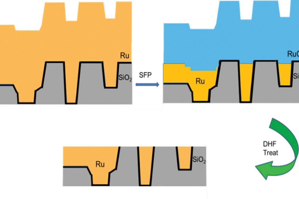
Figure 1. Stress-Free Polish and HF Etch Process Flow.
A different process technology is needed to more easily
integrate Ru into the interconnect process. This article details an integrated
stress-free polishing (SFP) and wet etching process developed as a novel
solution for efficient Ru removal to eliminate some of the above challenges. By
using an electrochemical reaction mechanism, the SFP step modifies the Ru
surface to form a thin ruthenium oxide (RuO2) layer. This oxide
layer can be readily etched by hydrofluoric acid (HF) solution.
Because Ru is essentially inert in HF, there is excellent
selectivity between Ru and RuO2; an optimized process demonstrates
this high removal selectivity. Moreover, the absence of mechanical stress,
abrasive particles and chemical components from the CMP slurry during the
process is expected to significantly minimize associated defects and potentially
improve yields. The proposed SFP–wet etch integration reveals strong potential
to serve as a replacement for conventional CMP in advanced-node Ru interconnect
fabrication, offering etch rates and selectivity that will meet the
requirements of advanced interconnect processes.
Emerging Ruthenium removal solution
An SFP technology using an electrochemical reaction mechanism was applied to treat the Ru surface and form a RuO2 film, which was then etched by HF, while the metallic Ru, which has a significantly lower etch rate in HF, was barely affected. By carefully controlling the electrochemical reaction, the thickness of the RuO2 can be controlled, removing the RuO2 and resulting in a planar surface. The integrated process flow consisted of oxidizing the Ru and a stress-free polish with a HF etch, all processed sequentially in the same chamber (Figure 1).

Figure 2. Stress-Free Polish Mechanism.
Figure 2 shows the experimental setup for the SFP. The wafer
is fixed on a chuck, which carries the wafer and can be moved horizontally and
vertically, along with the rotational movements typically used in a CMP
process. The thickness of the RuO2 is controlled by electrolyte
property, process current, wafer rotation speed, horizontal movement speed and
electrolyte flow rate.
The process conditions can be optimized for the formation of
the RuO2. The absence of mechanical stress, abrasive particles and
chemical components typically found in a CMP slurry process is expected to
significantly reduce defects on the wafer surface.
Two different samples were prepared for the experiments.
Silicon wafers with a 200nm Ru layer were diced into approximately 4cm x 4cm
pieces for the preliminary tests. Each piece was affixed to a 300mm blanket Cu
wafer at a radial position of 75mm from the wafer center using conductive Cu
tape. The samples were subjected to a sequential SFP and diluted HF (DHF)
cleaning process. To create a reference surface, the left half of each Ru piece
was masked with a piece of rectangular tape to prevent polishing.
The second set of samples for the experiment were Si wafers
coated with a Ru layer. This sample set also had tape covering a small part of
the surface at a similar location as the first experiment, with a radial
position of 75mm. The experimental process formed a step height between the
masked and unmasked regions.
A stylus profilometer was used to measure the resulting step height, and the Ru removal rate was calculated accordingly. The ESP9000 chemistry developed for the experiment was used as the polishing electrolyte with a flow rate of 32 LPM from the main nozzle (see Figure 2). The wafer was rotated at a speed of 100 RPM. The varying constant voltage of 0, 50, 100 and 200V was applied, respectively, for four samples with a polishing time of 60 seconds. The DHF cleaning/removal process used a solution of 3 %wt. DHF at a flow rate of 1.5 LPM for 120 seconds.

Figure 3. Removal Thickness vs. SFP Process Voltage.
Test results and insights
The results of the first set of experiments using diced Ru
samples on a blanket Cu wafer are shown in Table 1. Upon removal of the tape,
which prevented polishing the Ru, the stylus measurements gave the following
results. The baseline sample with no voltage applied and no SFP demonstrated
only 99Å of Ru removal. When 50V was applied with the SFP, there was also very
little removal, with only 90Å of Ru removed. The higher voltages of 100V and
150V, combined with SFP, resulted in higher etch rates of 959.2Å and 1336Å,
respectively. Figure 3 shows the step profiles of the first set of samples
using diced Ru chips on a 300mm Cu wafer.
Because Ru is relatively inert in HF, sample 1 had minimal
etching, as was expected. Increasing the voltage to 50V and adding the SFP also
showed limited etching, as the voltage was not strong enough to induce the
electrochemical reaction to form significant RuO2 on the wafer
surface. The higher voltages of 100V and 150V, respectively, demonstrated
oxidation of the Ru film and the subsequent etching of the RuO2
layer. Based on these results, it was concluded that the Ru layer had a very
limited reaction with the HF etch, making it an effective etch-stop layer
between the RuO2 and the Ru. Hence, the Ru removal is equal to the
oxidized RuO2 thickness during the SPF process.
In the second sample set, the voltage was increased to 200V
to maintain a higher level of current density due to the larger surface area
that needed to be polished. After a 120-second SFP, the measured step height
was 1820.9Å and 1814.8Å between the polished and unpolished areas on the
selected sample, respectively. This demonstrates that a Ru removal rate of more
than 15 Å/s can be achieved, which would be acceptable for a
manufacturing-worthy process with a blanket Ru deposition across the wafer.
The formation of the RuO2 is primarily controlled
by the voltage and the electrolyte applied to the wafer surface during the SFP.
From the thicknesses that were obtained, the higher the voltage, the faster the
formation of RuO2, and thus the higher the etch rate when exposed to
HF. Figure 4 shows Ru removal on a 300mm wafer.
Ru/SiO2 removal selectivity
The Ru interconnect structure also includes a SiO2
layer that is used as an insulator under the interconnect and is used for
defining the structure in the interconnect regions. Many times, this material
is a low-k SiO2 to improve the resistance capacitance properties of
the transistor. Because SiO2 is readily etched by HF, it was
critical to evaluate the selectivity between the SiO2 and the RuO2.
To do so, a series of experiments was designed to look at different HF
concentrations on RuO2 and SiO2 during the SFP process
using the same conditions as the above experiments.
As Table 2 illustrates, the higher the concentration of HF, the higher the etch rate of the SiO2 layer. The SiO2 also etches faster than the RuO2. Thus, the HF used in the process will need to be of a lower concentration to achieve the optimum selectivity and etch rate for the Ru-removal SFP process.

Figure 4. Removal Thickness for the Whole Ru Wafer.
Figure 5 shows the Pourbaix (potential-pH) diagrams for Cu
and Ru in aqueous solution, which illustrate how the different Cu and Ru oxides
form with varying pH and electrode potential. Copper readily forms oxides or is
dissolved to ionic species over a wide pH range, even at relatively low
electric potentials. Ru, however, is markedly inert; the formation of an oxide
requires much higher potentials, and direct dissolution of Ru (in the form of
RuO4-) occurs only under restricted conditions.
This is why common oxidizers in CMP slurries struggle to oxidize Ru and why it is challenging to remove using conventional CMP processing. It also highlights the advantage of applying a voltage during the SFP to deliberately regulate RuO2 formation and its subsequent removal in the SFP process.

Figure 5. Potential-pH Equilibrium Diagram for Cu-H2O
and Ru-H2O Systems at 25°C.
During the SFP using the external bias, the obtained
Ru(III), Ru(IV) or Ru(V) oxides and hydroxides react with DHF to form soluble
species, Hx [RuF6], through reactions 1–5 below. The ruthenium oxides are
carried away by the solution flow, efficiently removing the oxidized material.
Meanwhile, the underlying metallic Ru remains intact because
DHF alone cannot oxidize and react with the inert Ru, allowing the film-removal
thickness to be precisely controlled within the integrated process parameter.
The integrated process uniformly and efficiently removes the
oxidized Ru, leaving a uniform Ru surface. By adjusting the HF dilution levels,
the selectivity between the RuO2 and the SiO2 insulation
layer can be optimized to leave a uniform surface. The lack of abrasives could
minimize defects and result in higher yields.
Future outlook of advanced-node ruthenium interconnect
fabrication
In this work, an integrated process of SFP and HF wet etch
was developed as an emerging stress-free Ru-removal solution. Through the
optimization of process parameters of voltage, electrolyte and HF
concentration, the rapid removal of Ru on Si wafers of more than 1800Å within
120 seconds was achieved. Furthermore, by fine-tuning the DHF concentration, a
high removal selectivity between Ru and SiO2 was also realized. The
proposed SFP–wet etch integration demonstrates strong potential as a
replacement for conventional CMP in advanced-node Ru interconnect fabrication
and has the potential to minimize defects due to the absence of mechanical
stress, abrasive particles and chemical components from the CMP slurry.