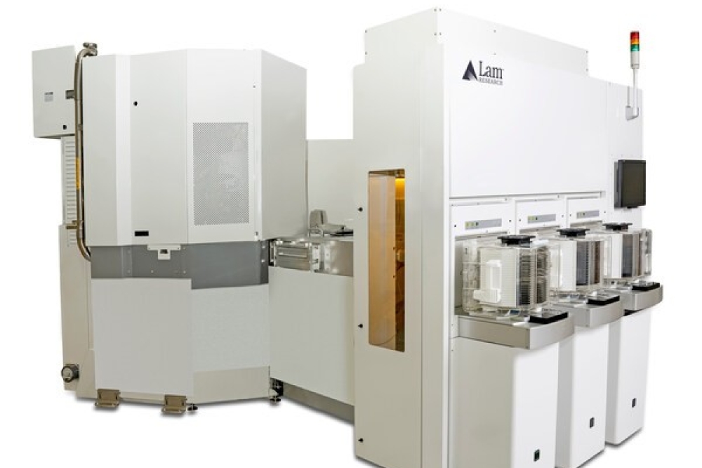
Lam Research unveils 'most advanced' Conductor Etch Technology
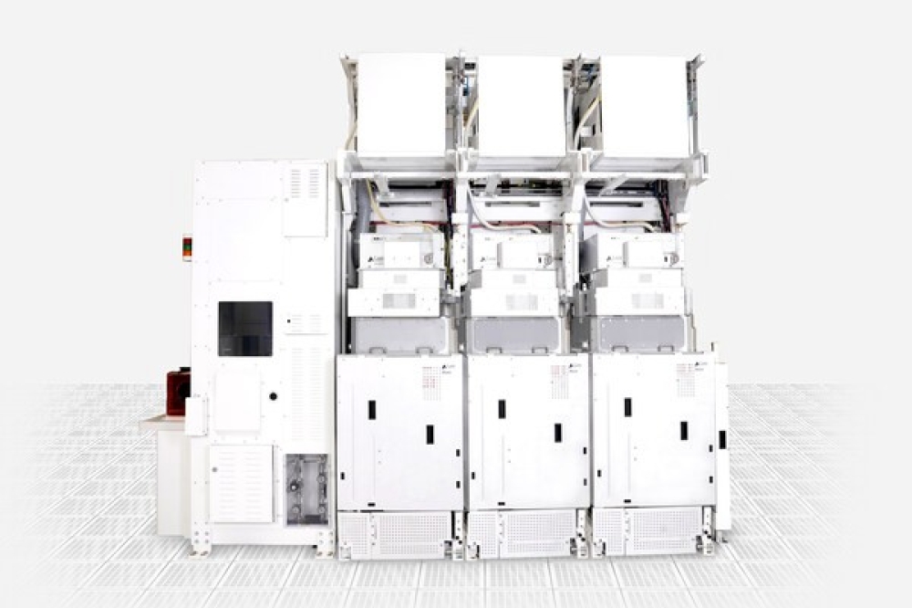
Lam Research has introduced Akara®, a breakthrough innovation in plasma etch and the most advanced conductor etch tool available.
Akara delivers novel plasma processing technologies that enable the 'unmatched' etch precision and performance needed for 3D chipmaking. Akara joins Lam's differentiated product portfolio that empowers chipmakers to overcome the industry's hardest scaling challenges.
"Building on more than 20 years of continuous conductor etch innovation, our groundbreaking new Akara etcher leverages Lam's proprietary DirectDrive® technology to deliver the controlled creation of atomic-scale features with plasma responses that are 100x faster," said Sesha Varadarajan, senior vice president of the Global Products Group at Lam Research. "Akara is a generational leap forward in conductor etch capabilities for shaping small, complex structures for the 3D era of chips."
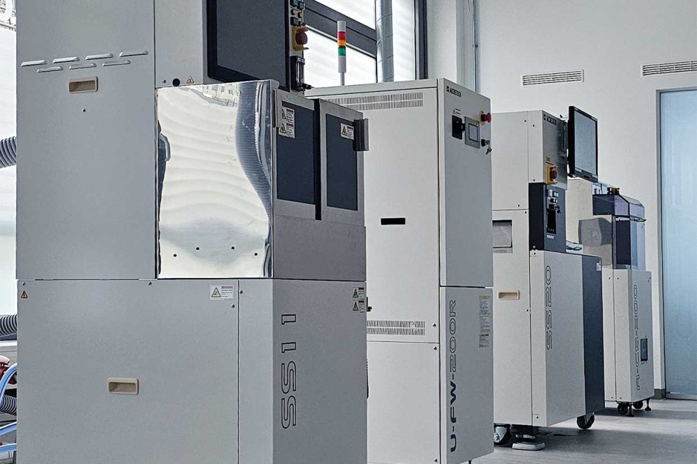
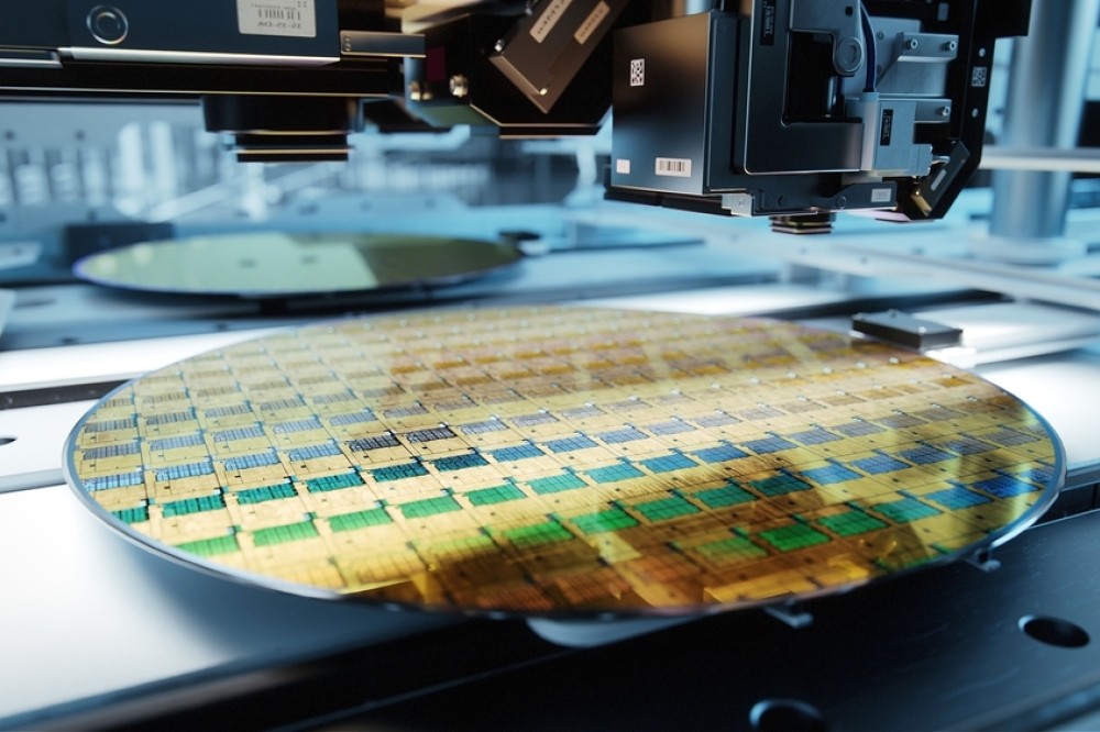
Lam Research Akara conductor etch
Akara extends decades of Lam leadership in conductor etch. This includes multiple generations of the company's highly successful Kiyo® conductor etch tool, which was introduced in 2004 and now has more than 30,000 chambers in production.
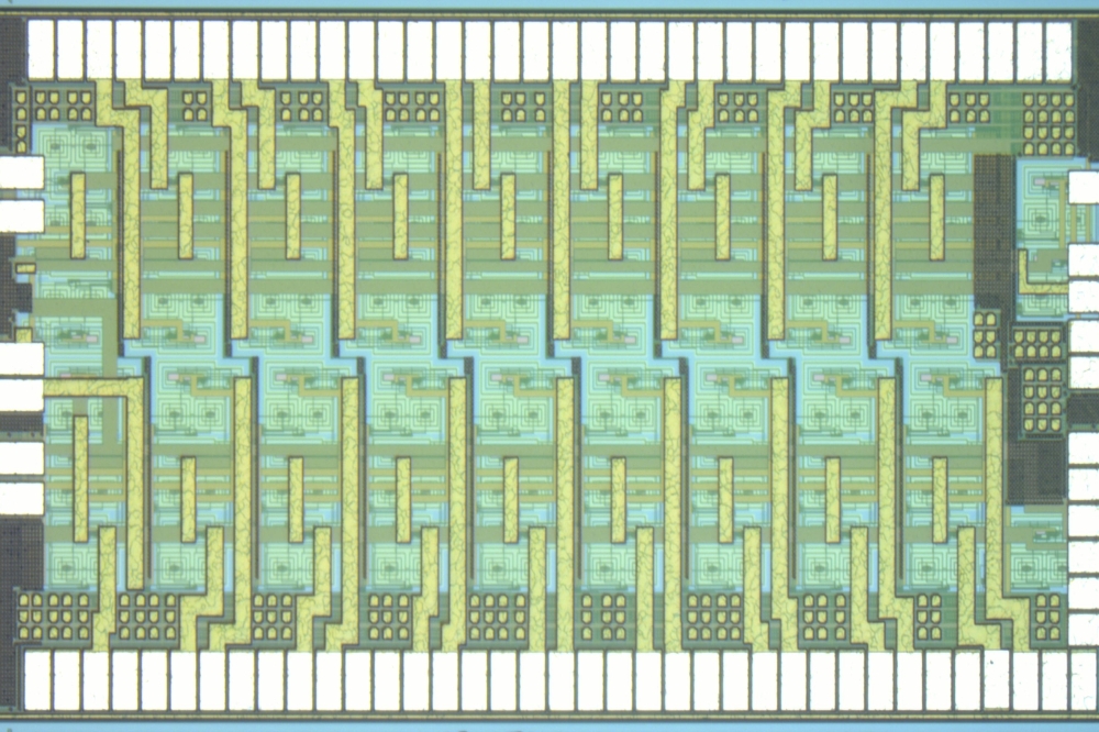
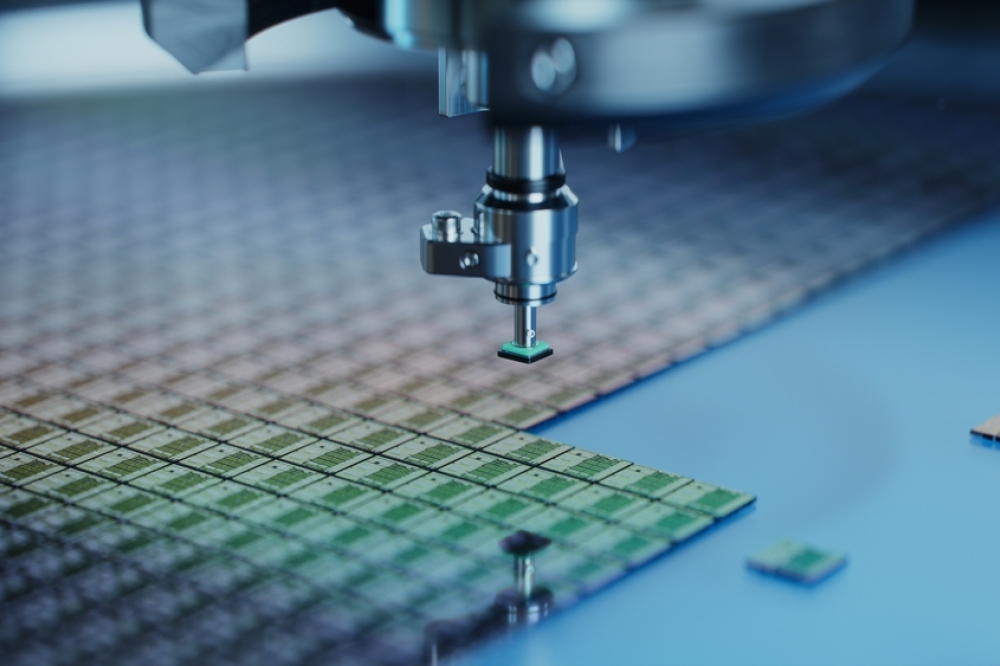
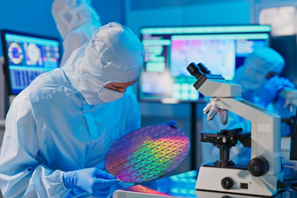
Akara enables the scaling of gate-all-around (GAA) transistors and 6F2 DRAM and 3D NAND devices, and is extendible for 4F2 DRAM, complementary field effect transistors, and 3D DRAM. These devices require challenging critical etch steps and precise Extreme Ultraviolet (EUV) lithography patterning to form complex 3D structures. Angstrom-level precision is required to create small features with progressively higher aspect ratios — beyond the current capabilities of mainstream plasma etch technologies.
"As global demand for semiconductors continues to grow, innovative technology solutions from our partners are required to enable new, more powerful device architectures," said Dr. Y.J. Mii, executive vice president and co-chief operating officer at TSMC. "Critical plasma etch capabilities will be an integral part of solving the many production challenges these new devices pose."
Akara leverages proprietary etch solutions invented by Lam to tackle these issues.
• DirectDrive, the industry's first solid-state plasma source, generates plasma with 100x faster responsiveness than previous sources, resulting in fewer EUV patterning defects.
• TEMPO plasma pulsing, a unique capability to control plasma species, provides new levels of etch selectivity and microloading performance.
• SNAP is a leading-edge ion energy control system that shapes etch profiles with atomic precision.
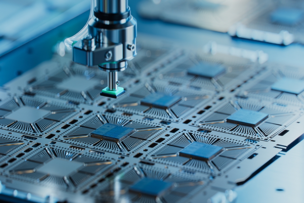
Designed for high-volume production with maximum process yield, Akara optimizes wafer output with millisecond response times. Sophisticated etch uniformity controls ensure wafer-to-wafer repeatability. Integrated on Lam's high-productivity Sense.i® platform, Akara leverages Equipment Intelligence® solutions for automated maintenance to reduce overall equipment upkeep. Together, these features enable chipmakers to drive greater value from their manufacturing equipment.
Akara has been selected by leading device manufacturers as production tool of record for multiple, advanced planar DRAM and foundry GAA applications. Its value has been validated by these customers with repeat orders and a rapidly growing installed base.
The introductions of Akara and the separately announced ALTUS® Halo, the world's first molybdenum atomic layer deposition tool in production, further demonstrate Lam's focus on delivering innovations needed to ensure chipmakers are ready for upcoming semiconductor inflections.