Lam Research ushers in new era of semiconductor metallisation
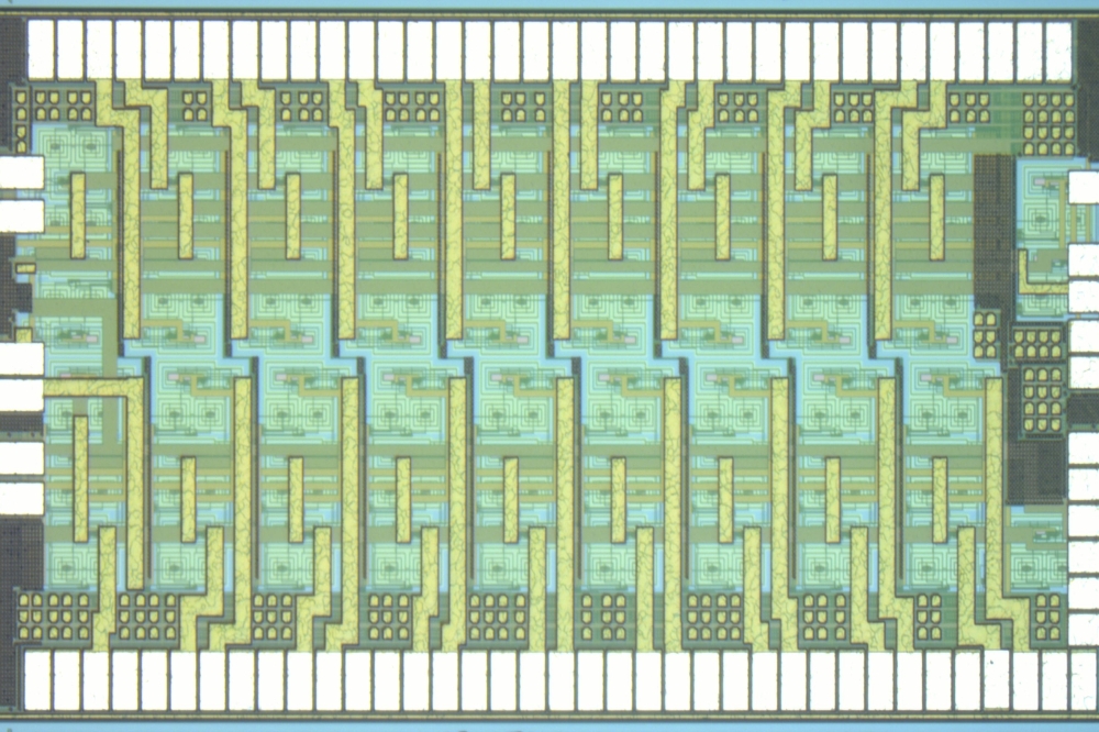
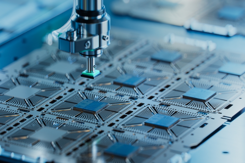
Lam Research has unveiled ALTUS® Halo, said to be the world's first atomic layer deposition (ALD) tool that harnesses the capabilities of the metal molybdenum in the production of leading-edge semiconductors.
Leveraging a range of patented innovations, ALTUS Halo delivers exceptional feature fill and high-precision deposition of low resistivity, void-free molybdenum metallization for advanced semiconductor devices. Currently in qualification and ramping with all leading chipmakers, ALTUS Halo represents the tipping point in a new age of semiconductor metallization, paving the way for future scaling of advanced memory and logic chips for tomorrow's AI, cloud computing and next-generation smart devices.
ALTUS Halo is the newest addition to Lam's ALTUS product family and is part of a differentiated product portfolio that enables chipmakers to overcome some of the industry's hardest scaling challenges. It joins Akara®, the most advanced conductor etcher available, which was announced separately today by Lam Research.
ALTUS Halo Harnesses the Potential of Molybdenum
As the performance demands of next-generation applications increase, so does the need for more advanced semiconductors and new manufacturing processes to create them. The atom-by-atom deposition of metal is essential in the manufacturing of all leading-edge chips today. Tungsten-based ALD, first pioneered by Lam, has been the predominant metallization technique for deposition and void-free fill of contacts and lines for over two decades. However, to scale NAND, DRAM and logic devices for the future, chipmakers will need to shift metallization beyond what is currently possible with tungsten integration. With ALTUS Halo, Lam is taking a leadership role in the semiconductor industry's transition from tungsten to molybdenum.
"Building on Lam's deep metallization expertise, ALTUS Halo is the most significant breakthrough in atomic layer deposition in over 20 years," said Sesha Varadarajan, senior vice president and general manager of the Global Products Group at Lam Research. "It brings together Lam's quad station module architecture and new advancements in ALD technology to provide engineered, low-resistivity molybdenum deposition for high-volume manufacturing — a critical requirement for emerging and future chip inflections, including 1,000-layer 3D NAND, 4F2 DRAM and advanced gate-all-around logic."
Molybdenum Enables Low-Resistance Metallization Required for Next-Generation Chips
For semiconductors to operate, fast electrical signals travel through connections, such as 3D NAND wordlines, to send commands. Nanoscale features are etched and, when copper cannot be used, they are traditionally filled with tungsten to create the essential connections. The lower the metal resistivity, the faster the signal speeds. Additionally, in conventional tungsten-based wiring, extra barrier layers are added to prevent unwanted electrical interactions. As NAND, DRAM and logic scale to more complex architectures including 3D integration, electrical signals must travel through more restrictive connections. This increases the potential for bottlenecks and slower speeds, and the possibility of electrical shorts in some instances.
Molybdenum is an ideal metal for these and future applications because it has lower resistivity in nano-scale wires than tungsten and doesn't need an adhesion or barrier layer, thereby reducing the number of process steps, boosting efficiency and helping improve chip speed. Building on decades of expertise in metallization and advanced development, and through new innovations in deposition technology, Lam has made the ALD of molybdenum viable for mass production for the first time. In most instances ALTUS Halo provides better than 50% improvement in resistance over conventional tungsten metallization.
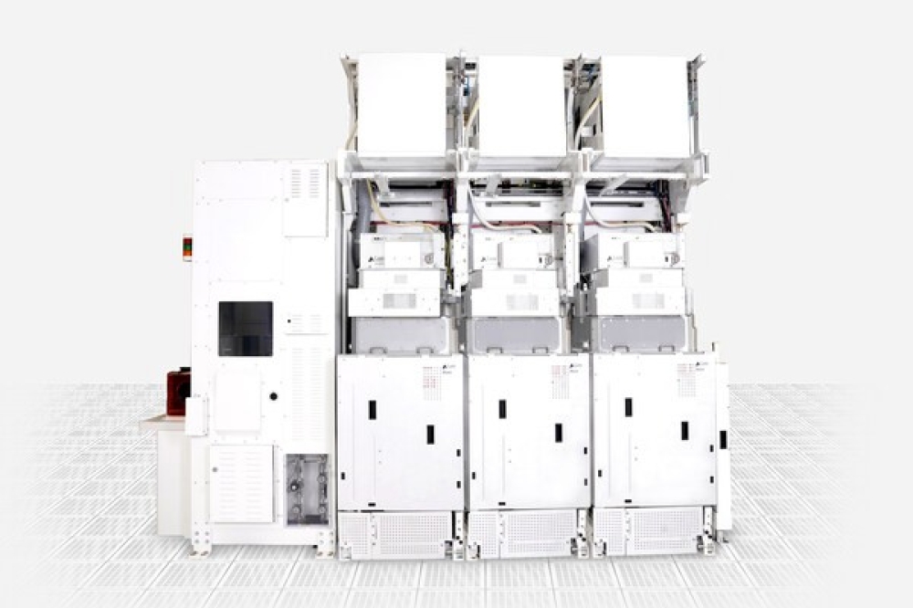
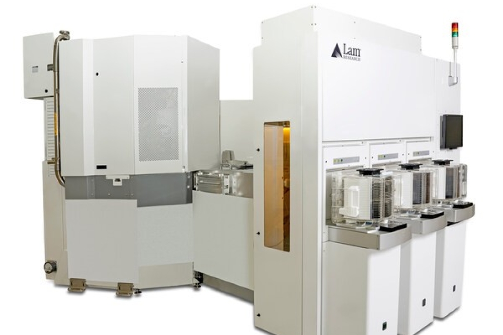
ALTUS Halo is in Volume Production
ALTUS Halo is designed to deliver the most precise and advanced deposition of molybdenum in the semiconductor industry. The ALTUS Halo tool series is optimized for a range of metallization needs, with the ability to deposit conformally or selectively with bottom-up feature fill using chemistry and thermal flexibility, as well as plasma for temperature-sensitive applications.
Early adoption has begun at leading high-volume 3D NAND manufacturers with fabs in Korea and Singapore and in advanced logic fabs, while development continues with DRAM customers.
"The integration of molybdenum metallization enables Micron to be first to market with industry-leading I/O bandwidth and storage capacity in the latest generation of NAND products," said Mark Kiehlbauch, corporate vice president of NAND development at Micron. "Lam's ALTUS Halo tool has made it possible for Micron to bring molybdenum into mass production."