Park Systems Expands FX Large Sample AFM Lineup to Power Next-Gen Industrial Innovation
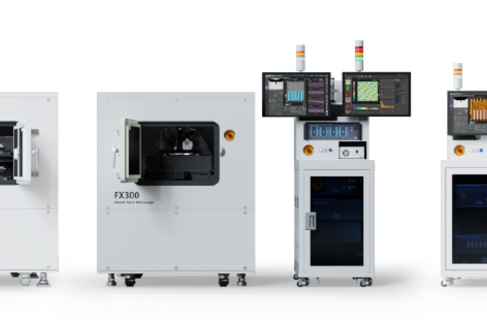
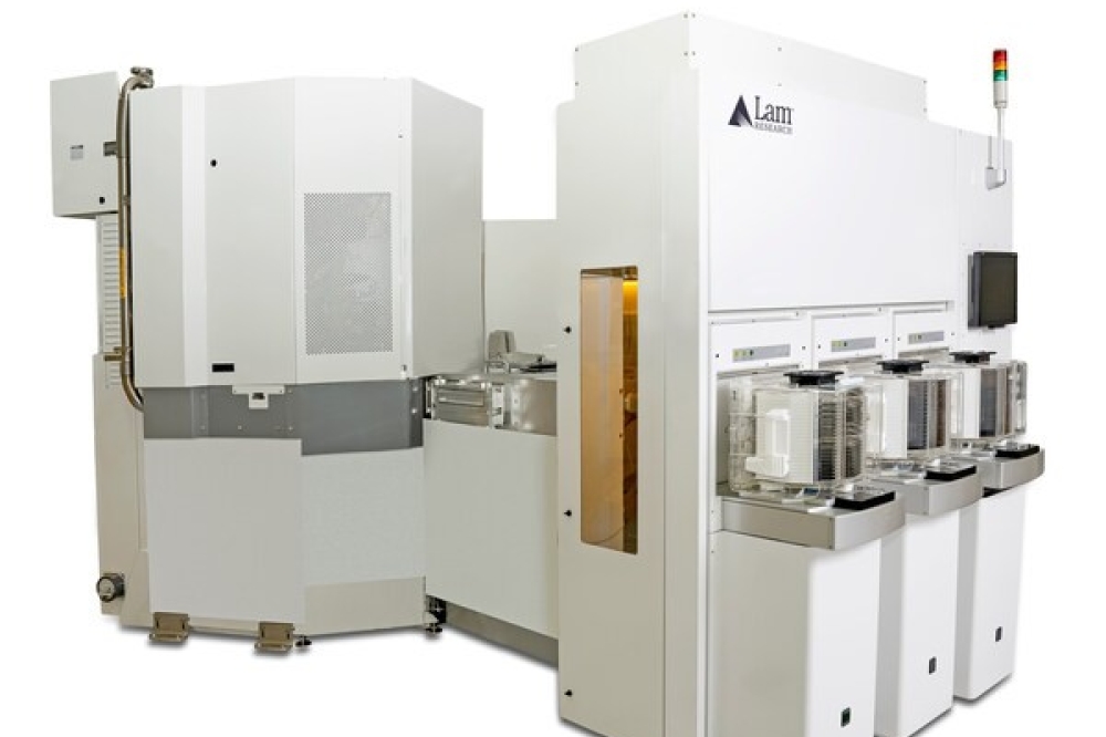
Park FX Large Sample AFM Series: From left, FX200 IR, FX300, and FX300 IR
Park Systems, in atomic force microscopy (AFM), has unveiled an expanded FX Large Sample AFM series at SEMICON Korea 2025. Building on the success of Park FX200, which debuted at SEMICON West 2024 and has since gained strong market traction in Germany, Japan, and Korea, Park Systems introduces Park FX300 for 300 mm wafer analysis, alongside Park FX200 IR and FX300 IR, which integrate infrared (IR) spectroscopy, pushing the boundaries of large-sample AFM technology.
As 300 mm wafers become the semiconductor industry standard, the Park FX300 is designed for those seeking high-precision analysis without the complexity of a fully automated inline system. It also serves as an ideal solution for companies considering AFM implementation before transitioning to inline fabrication.
Optimized for both industrial and research applications, the Park FX300 is expected to be a game-changer, delivering advanced capabilities for analysis and quality control across a wide range of AFM techniques. It is equipped with specialized features such as a Sliding Stage for long-range flatness measurements of copper pads in semiconductor post-processing, a Rotation Stage for precise sample alignment in wafer-level packaging, and an Off-Axis Optics system for enhanced sample visualization. Additionally, its Fan Filter Unit (FFU) ensures a controlled, contamination-free environment, making it ideal for cleanroom applications.
Park Systems has also introduced FX200 IR and FX300 IR, expanding its AFM technology into the realm of nanoscale chemical analysis. By integrating Fourier Transform Infrared Spectroscopy (FTIR) with AFM, these models utilize Photo-induced Force Microscopy (PiFM) to enable chemical identification with a spatial resolution less than 5 nm. This breakthrough allows researchers and engineers to analyze the chemical composition of nanoscale structures without damaging wafer surfaces, opening new possibilities for material characterization in semiconductor, polymer, and life science applications.
Designed for samples ranging from small sizes to 200 mm or 300 mm wafers, the FX200 IR and FX300 IR enable high-resolution infrared spectral imaging, providing unprecedented insights into material composition and molecular interactions. With its ability to capture chemical bonding information at an ultra-fine scale, it enhances semiconductor defect analysis, polymer research, and advanced material characterization with unmatched precision.
Rooted in Park Systems’ philosophy of maximizing efficiency while minimizing manual intervention, the FX Large Sample AFM series enhances usability with automated probe recognition and exchange, a QR code system for probe status monitoring, and AI-driven laser alignment for seamless operation. The StepScan™ function further boosts efficiency by enabling automated sequential measurements at predefined coordinates, allowing researchers to analyze topography, electrical, mechanical and magnetic properties with minimal manual intervention. Especially in IR applications, where laser alignment is often a significant challenge, the systems fully automates the process, making high-resolution chemical analysis more accessible than ever before.
Dr. Sang-Joon Cho, Executive Vice President of Park Systems, emphasized the company’s commitment to technological leadership: “Embodying Park Systems’ decades of expertise and innovation in precision measurement and automation, we have optimized the FX Large Sample AFM series for wafer analysis at the highest level for both industrial and research fields. Park FX300 and the nano-IR systems are redefining the boundaries between industrial and research AFM applications, empowering our customers with the most advanced AFM available—shaping the future of nanoscience together.”
With its latest innovations, Park Systems continues to solidify its position as a global leader in atomic force microscopy, providing industry-leading solutions for the ever-evolving demands of semiconductor and nanoscience research.