Baya Systems 'revolutionises' AI scale-up and scale-out

Breakthrough in data movement enables 100x node density and scale, surpassing present-day systems for next-generation AI with high-density switching.
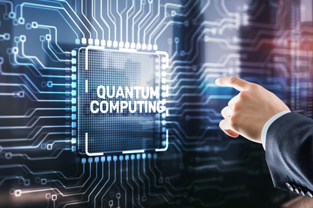
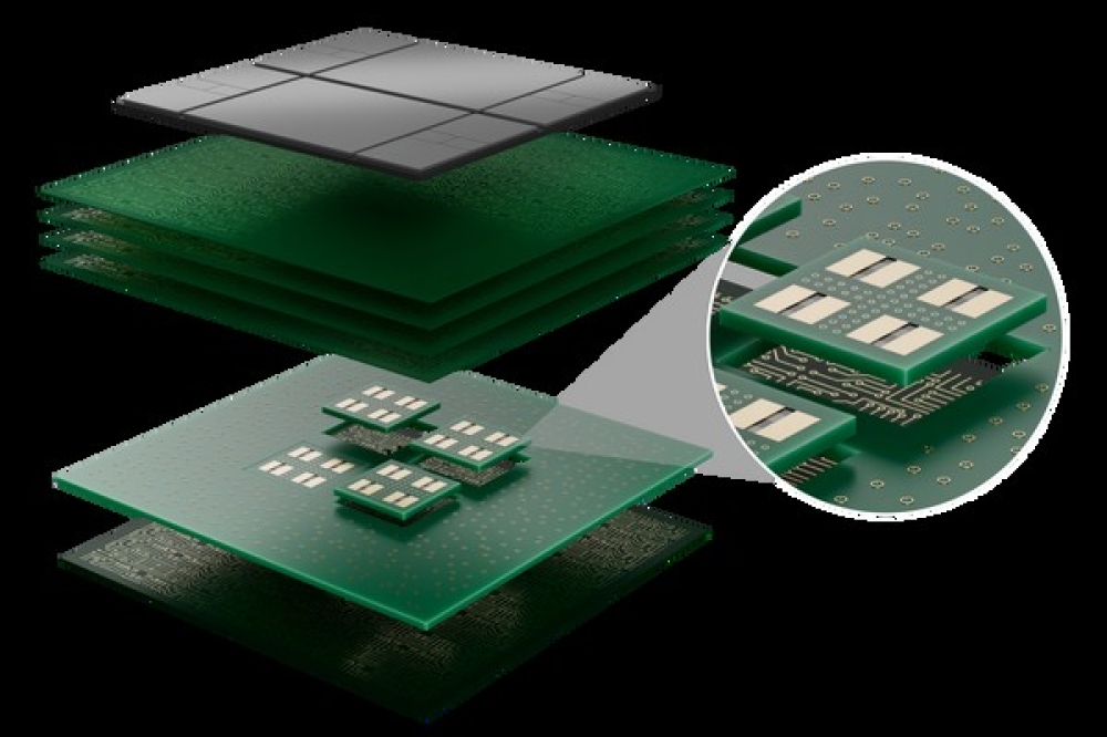
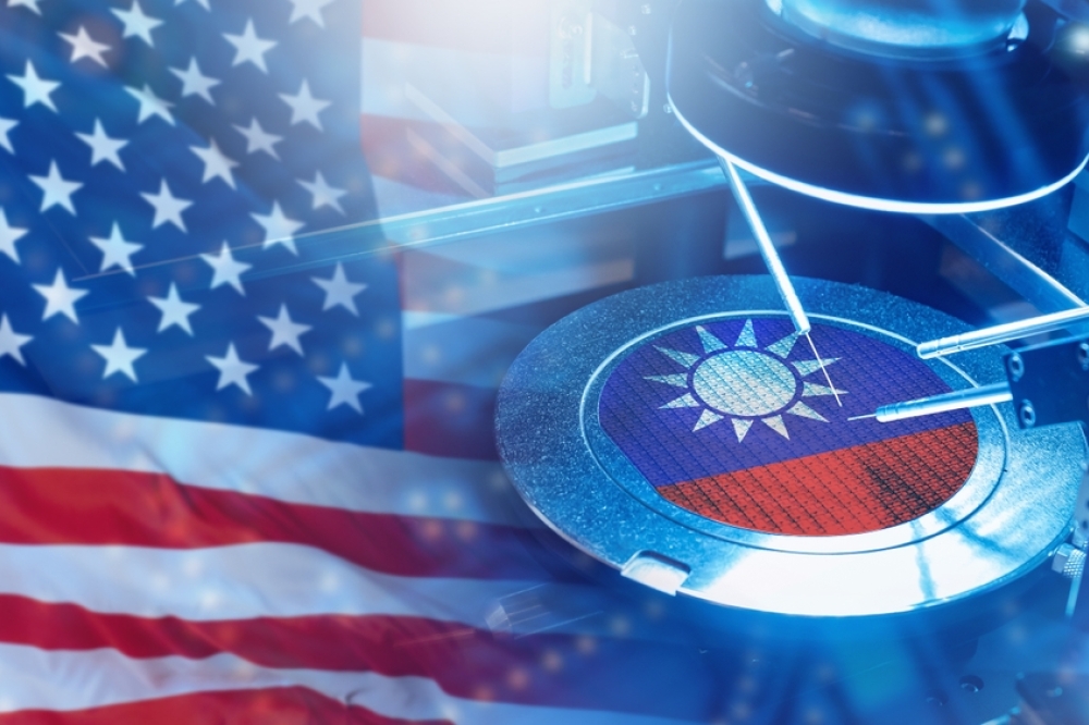
Baya Systems has introduced its new NeuraScale™ switch fabric technology designed to overcome critical scaling and data movement challenges in AI infrastructure that are driving advanced SoCs and emerging 3D chiplet-based designs. As AI workloads demand unprecedented levels of performance, throughput and efficiency, traditional crossbar switching architectures are struggling to keep pace. NeuraScale provides a radical and fresh approach, delivering non-blocking performance to enable a 100x increase in node density and scale that will substantially outperform today’s platforms.
"NVIDIA has demonstrated the benefits of high-performance networking for scaling AI with its NVLink™ proprietary interconnect,” said Karl Freund, founder of Cambrian-AI Research. “Now the industry is developing the UALink™ standard, which could democratize scaling, but it needs rapid innovation in SoC and chiplet-ready switching technologies creating opportunities for companies like Baya Systems and their fabric solutions.”
A Breakthrough in AI Infrastructure Scaling
While NVLink, UALink and Ultra Ethernet have advanced interconnect technology, the industry still faces fundamental limitations in scaling performance and density. Baya Systems’ patent-pending NeuraScale switch fabric introduces a fundamentally new approach that pushes beyond the constraints of conventional switching architectures, enabling next-generation AI systems to achieve unparalleled levels of efficiency, speed, and scalability.
Radical Scalability: Supports 256 ports per chiplet with 1 Tb/s throughput, enabling next-generation AI infrastructure.
Unprecedented Performance: Achieves 2 GHz+ operation in 4 nm technology with less than 20 ns maximum latency and 2048-bit data width for efficient data transfer.
Modularity for chiplets: A fully modular architecture that simplifies physical implementation for each SoC, while enabling seamless scaling across multiple chiplets.
Protocol-Ready for Industry Standards: Supports AMBA protocols and is designed for future UALink, UCIe and Ultra Ethernet compliance.
“The Ultra Accelerator Link™ Consortium (UALink™) was formed with a vision of creating an open ecosystem that boosts innovation and collaboration in scale-up, and our first specification will support up to 1K accelerators in an AI pod,” said Peter Onufryk, President of the UALink Consortium. “We welcome Baya Systems, which joins a rapidly growing set of game changers meeting the challenges of AI scaling.”
When combined with Baya Systems’ WeaverPro, a software-driven platform that streamlines design, analysis and KPI-driven optimization, NeuraScale significantly accelerates development cycles. It simplifies large-scale interconnect implementation, overcoming key bottlenecks in traditional crossbar architectures, while offering flexible, multi-protocol support to ensure interoperability and adaptability for AI-driven data centers.
"AI workload demands have outpaced what traditional crossbar interconnects can provide for the next generation of scale-up," said Dr. Sailesh Kumar, Baya Systems' CEO. "NeuraScale empowers a radical growth in node density, with highly energy-efficient and area-efficient switching solutions for next-gen AI – the key challenges to scale. With our platform, we enable unprecedented performance and scale, while substantially reducing the implementation challenges and time to market, which are serious challenges for traditional switching solutions.”