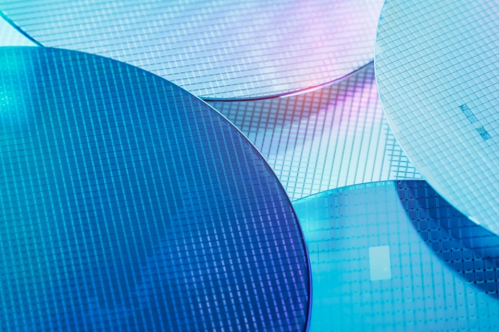
Marvell demonstrates leading 2nm silicon for accelerated infrastructure

The Marvell® 2nm platform will enable hyperscalers to dramatically boost the performance and efficiency of their infrastructure to meet the performance and efficiency demands of the AI era.
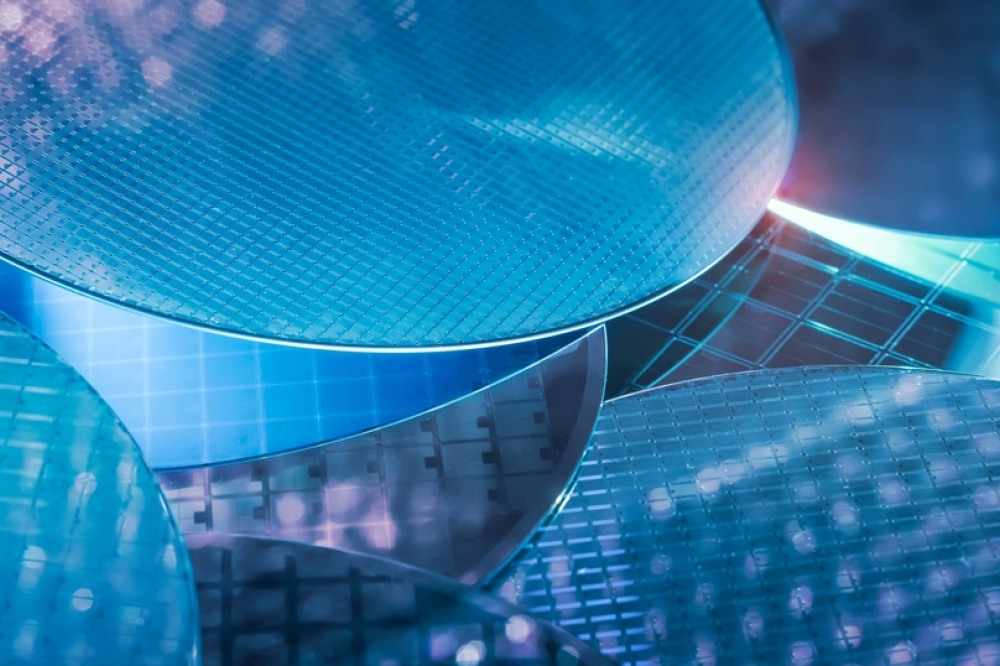
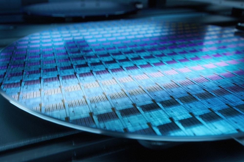
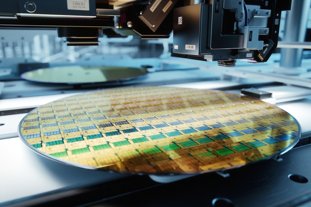
Marvell Technology has demonstrated its first 2nm silicon IP for next-generation AI and cloud infrastructure. Produced on TSMC's 2nm process, the working silicon is part of the Marvell platform for developing custom XPUs, switches and other technology to help cloud service providers elevate the performance, efficiency, and economic potential of their worldwide operations.
Given a projected 45% TAM growth annually, custom silicon is expected to account for approximately 25% of the market for accelerated compute by 20281.
A Building Block Approach
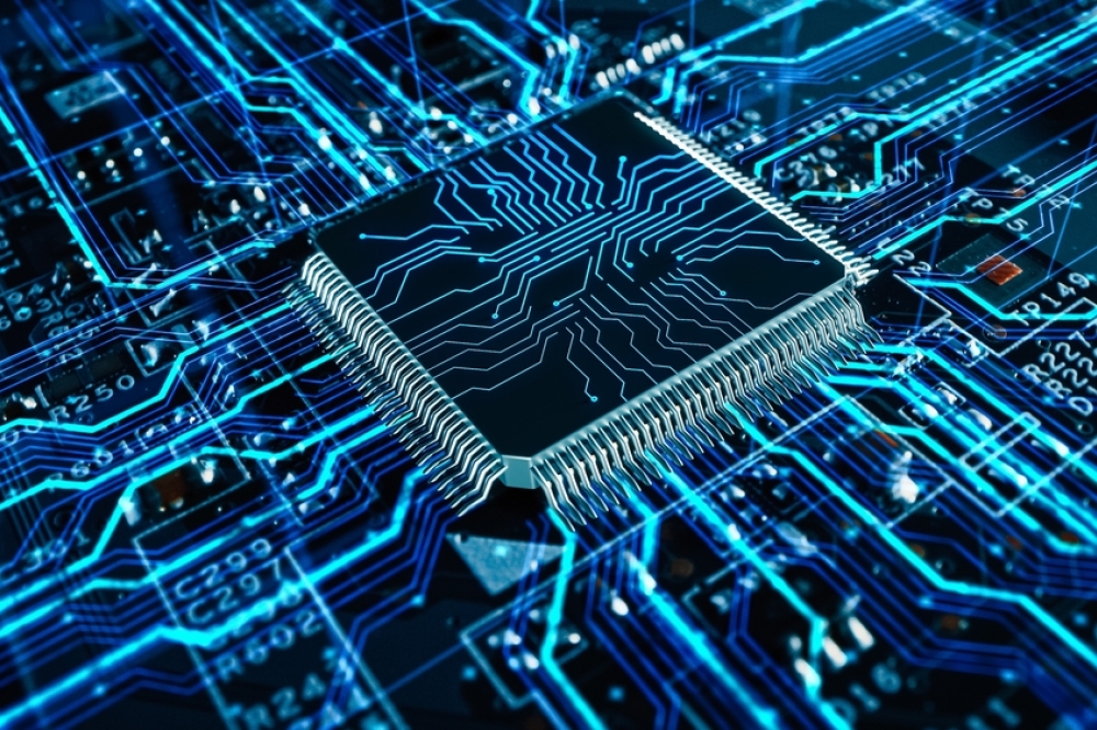
The Marvell platform strategy centers around developing a comprehensive portfolio of semiconductor IP—including electrical and optical serializer/deserializers (SerDes), die-to-die interconnects for 2D and 3D devices, advanced packaging technologies, silicon photonics, custom high-bandwidth memory (HBM) compute architecture, on-chip static random-access memory (SRAM), system-on-chip (SoC) fabrics, and compute fabric interfaces such as PCIe Gen 7—that serve as building blocks for developing custom AI accelerators, CPUs, optical DSPs, high-performance switches and other technologies.
Advanced Technology Leadership
Starting with the launch of the industry's leading 5nm data infrastructure silicon platform in 2020, Marvell has been at the forefront of developing products produced on advanced technology nodes to market. Marvell announced the industry's leading 3nm platform in 2022, with first silicon produced in 2023 and multiple industry standard and custom silicon products now shipping and in development.
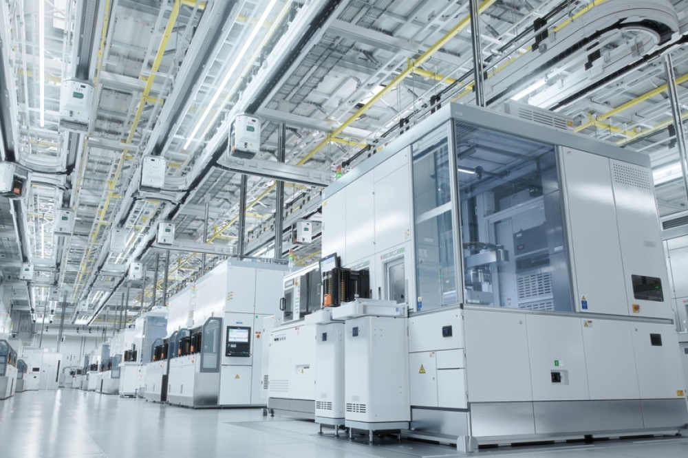
"The platform approach enables us to accelerate the development of market-leading high-speed SerDes and other critical technologies on the latest process manufacturing nodes, which in turn enables Marvell and its customers to accelerate the development of XPUs and other accelerated infrastructure technologies," said Sandeep Bharathi, chief development officer at Marvell. "Our longstanding collaboration with TSMC plays a pivotal role in helping Marvell develop complex silicon solutions with industry-leading performance, transistor density and efficiency."
New on the Marvell 2nm Platform
Additionally, Marvell delivered a 3D simultaneous bi-directional I/O operating at speeds up to 6.4 Gbits/second for connecting vertically stacked die inside of chiplets. Today, the I/O pathways connecting stacks of die are typically unidirectional. Shifting to a bi-directional I/O gives designers the ability to increase bandwidth by up to two times and/or reduce the number of connections by 50%.
3D simultaneous bi-directional I/O will also give chip designers greater flexibility in design. Today's most advanced chips exceed the size of the reticle, or photomask, for outlining transistor patterns onto silicon. To increase transistor count, an estimated 30% of all advanced node processors are expected to be based around chiplet designs, where multiple chips are combined into the same package2. With 3D simultaneous bi-directional I/O, designers will be able to combine more die into increasingly taller stacks for 2.5D, 3D and 3.5D devices that provide more capabilities than a traditional monolithic silicon device while still functioning like a single device.
"TSMC is pleased to collaborate with Marvell on the development of its 2nm platform and the delivery of its first silicon," said Dr. Kevin Zhang, senior vice president of business development and global sales, and deputy co-chief operating officer at TSMC. "We look forward to our continued collaboration with Marvell to utilize TSMC's best-in-class silicon technology process and packaging technologies to advance accelerated infrastructure for the AI era."