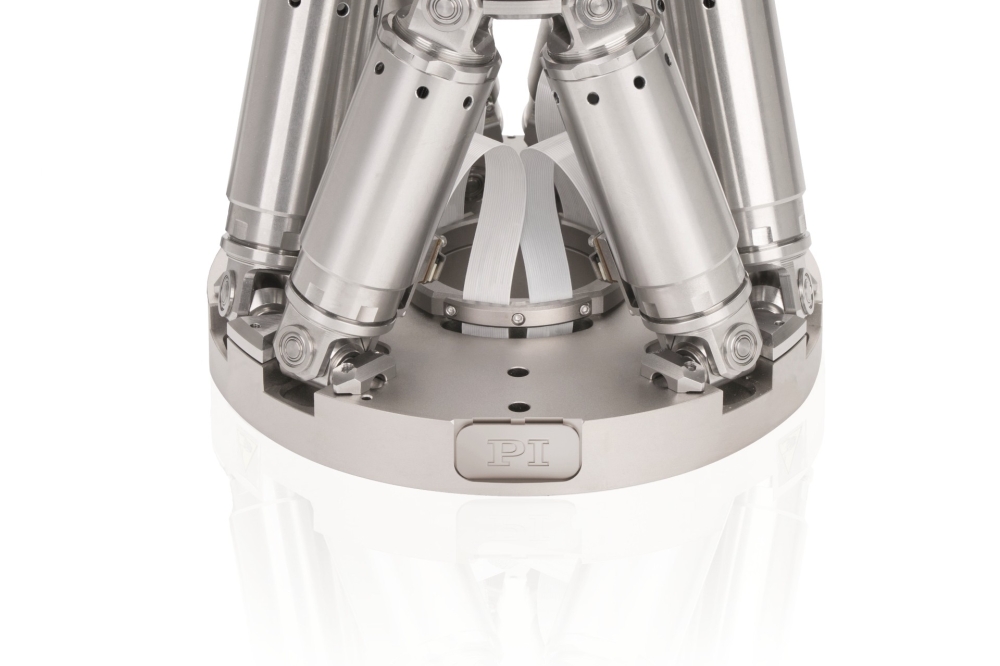
Laser annealing platform the logic choice

Two leading-edge logic customers have selected Veeco’s Laser Spike Annealing Platform as Production Tool of Record for new applications at their gate-all-around nodes. Veeco expects high-volume manufacturing orders tied to these wins as each customer ramps their advanced nodes.
“We continue to see growing adoption of our laser annealing platform for new applications as demonstrated by this announcement,” commented Adrian Devasahayam, Ph.D., Veeco’s Senior Vice President, Product Line Management. “Veeco's LSA system is widely acknowledged as the optimum annealing solution for low thermal-budget applications, and as device geometries and performance requirements at advanced nodes continue to evolve, precise annealing by our LSA platform has become increasingly critical. Both wins are a culmination of ongoing collaboration with each customer and validate Veeco’s strategy of expanding its Served Available Market by investing at the leading-edge.”
Laser spike annealing is a millisecond annealing technology used in front-end semiconductor manufacturing to lower the resistance of key transistor structures by activating dopants. Veeco’s LSA system is capable of high temperature annealing while staying within reduced thermal budgets of advanced devices at leading-edge nodes. Veeco’s Laser Annealing portfolio also includes its NSA500 system, which extends annealing capabilities to low thermal budget applications, like Backside Power Delivery and Contact Annealing for advanced nodes and material modification applications such as void-removal, recrystallization, and grain growth. These annealing steps are instrumental in determining the electrical properties and performance of the resulting devices.