Smart and compact sensors with Edge-AI

A newly launched interdisciplinary research project involving universities of Brandenburg and research institutions is developing new technological approaches for better and more effective integration of artificial intelligence at the edges of IT networks, so-called “edges”.
These developments could be of great importance in the future, particularly for applications in industrial electronics, medical technology and environmental monitoring. Fraunhofer IPMS is contributing its expertise in miniaturized sensor structures and the integration of electronic components.
In the project with the name “InSeKT” (German: Development of Intelligent Sensor Edge Technologies), the Technical University of Applied Sciences Wildau, the Leibniz Institute for High Performance Microelectronics (IHP) and the Fraunhofer-Institute for Photonic Microsystems IPMS are working on new hardware, software and sensor solutions to make better use of artificial intelligence (AI) right at the edges of IT networks. Artificial intelligence must process large amounts of data as quickly as possible. The aim of the project is to enable complex calculations directly where the data is generated, for example at the sensor itself.
Currently, data processing using AI is often carried out via central cloud computing solutions. The data is calculated on central servers, which means that large amounts of data are transmitted over long distances. As a result, data leaks can occur which creates opportunities for unauthorized third parties to attack. Decentralized data processing not only improves data protection, but also enables real-time capability of the systems, as data transmissions over long distances are avoided.
The project addresses the key factors for market acceptance: developing technologies for system integration, reducing costs, increasing reliability and increasing the degree of miniaturization. It is led by an interdisciplinary team from various institutions and specialist disciplines.
Advanced sensor technology to solve material and integration problems
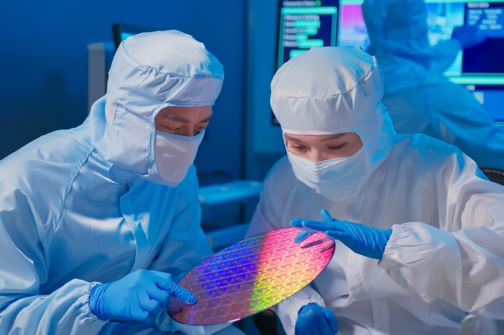
The Cottbus-based ‘Integrated Silicon Systems’ branch of the Fraunhofer Institute for Photonic Microsystems IPMS is working on the functional expansion and integration of existing MEMS sensors for edge AI applications. Signal processing is integrated directly into the sensor and data can be collected directly where it is generated. The aim is to increase the adaptability of sensors to different application scenarios without having to replace the underlying hardware.
An initial central area of development at Fraunhofer IPMS is gas analysis using ion mobility spectrometers (IMS). An IMS makes it possible to detect ionizable analyte substances directly in the air, even at very low concentrations. Existing approaches lack sufficient miniaturization. A first IMS demonstrator, which is based on a FAIMS (field asymmetric-waveform ion mobility spectrometry) approach, has flexible electrode spacing, making it possible to overcome this hurdle.
Furthermore, the goal of a data-supported evaluation of photodetectors for the near-infrared wavelength range is being pursued. These are used, for example, in material analysis and recycling and even enable analysis through packaging. The focus lies on improving an Al-TiN-Si-Schottky detector component with cylindric pyramidal structures for a higher sensitivity and improved scalability by using cheaper materials.
A third area deals with the adapted use of capacitive micromechanical ultrasonic transducers (CMUTs) for improved imaging. CMUTs are highly sensitive ultrasound receivers due to their size and capacitive operating principle. Signal evaluation close to the sensor would enable faster imaging. “Later on, it will be possible to carry out very precise analyses of hand movements using an ultrasound signal based on that of bats, as well as measuring blood sugar using ultrasound,” explains Dr. Sebastian Meyer, Head of the ‘Integrated Silicon Systems’ department at Fraunhofer IPMS.
The TH Wildau and the Leibniz IHP will then use the generated sensor data to train edge AI systems for fast and precise data processing. The results of the project will enable further steps towards more intelligent and compact sensor systems.