Loading...
News Article

ACM Research receives 2025 3D InCites Technology Enablement Award

News

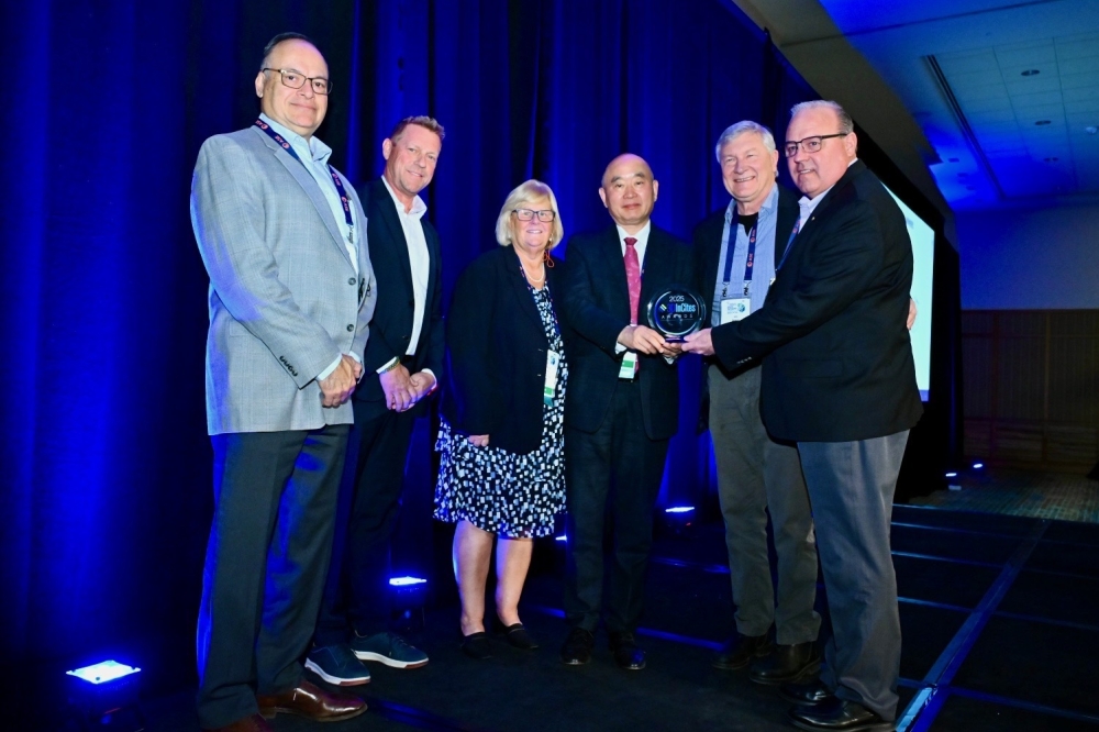
ACM Research's Ultra ECP ap-p tool has won the 2025 3D InCites Award in the Technology Enablement category.

This award honors companies that have identified and solved critical challenges in the advancement of the heterogeneous integration roadmap, driving the industry forward through cutting-edge solutions and advancements.

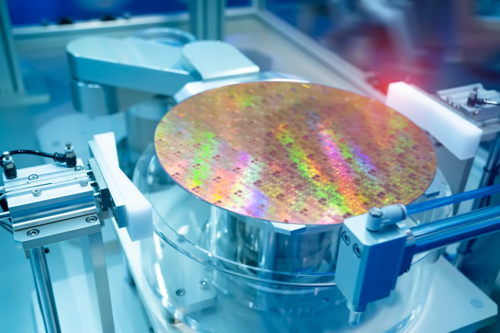
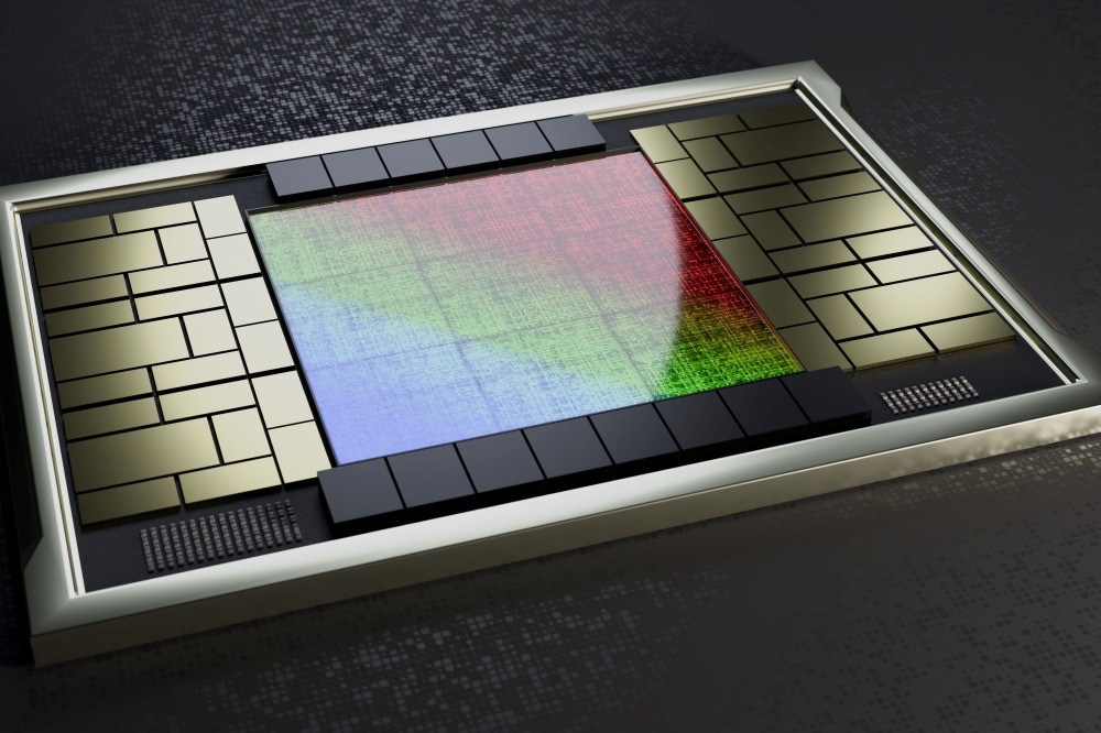
ACM’s Ultra ECP ap-p system, designed for fan-out panel-level packaging (FOPLP), is the first commercially-available high-volume copper deposition system for the large panel market. By using a horizontal plating approach, it achieves exceptional uniformity and precision across the entire panel. The tool supports 515 mm x 510 mm and 600 mm x 600 mm panel sizes and can be used for plating steps in a variety of processes including pillar, bump and redistribution layer.


“I believe this award recognition from 3D InCites validates ACM’s dedication to innovation in addressing customers’ challenges in panel-level packaging (PLP),” said Dr. David Wang, ACM’s President and Chief Executive Officer. “As the demand for large chiplets, high-performance graphics processing units and high-density high-bandwidth memory continues to grow, PLP has emerged as a key solution for reducing cost and improving efficiency. The Ultra ECP ap-p system is a vital addition to ACM’s expanding FOPLP portfolio, reinforcing our commitment to advancing high-volume manufacturing solutions.”

CE3S introduces Millice StripAid X Series
IDTechEx explores emerging applications for PICs
Miniature hexapod designed for demanding applications
ACM Research receives 2025 3D InCites Technology Enablement Award
ROHM develops low ON-resistance, high-power MOSFETs
Exploring packaging technologies
AI tops tech growth charts
Hailo selects Avnet ASIC as Channel partner for TSMC silicon production
Innatera appoints Intralink to bring brain-inspired AI to Asia
ABLIC strengthens semiconductor portfolio
Infineon bolsters global lead in automotive semiconductors
Infineon to acquire Marvell’s Automotive Ethernet business
Ansys semiconductor solutions certified by TSMC
InfiniLink secures $10M funding from MediaTek, Sukna Ventures, and Egypt Ventures
UMC unveils new fab facility in Singapore
Tokyo Electron and IBM renew collaboration
Production system for double-sided wafer probe test for silicon photonics
Imec pioneers photonic code-division multiplexing FMCW 144GHz distributed radar
Lightmatter unveils Passage M1000 Photonic Superchip
Onto Innovation and LPKF set to accelerate mass production of glass core substrates
Quantum sensors: from lab to chip through semiconductor fabs
SONOTEC attends European CMP and WET Users Group Meeting in Leuven, Belgium
iPronics unveils World’s silicon photonics optical circuit switch
Marvell demonstrates silicon photonics light engine
Baden-Württemberg attracts imec to lead development of chiplet-based technology
Europe’s semiconductor industry focuses on sustainable growth
Arteris opens new Engineering Hub in Poland
SONOTEC attends European CMP and WET Users Group Meeting in Leuven, Belgium
High-accuracy packaging in panel level packaging
ImageIR 6300: Cooled Thermographic Camera for Continuous Industrial Operation
PhotonDelta and Silicon Catalyst form strategic collaboration
Sarcina Technology launches AI platform
×
Search the news archive

To close this popup you can press escape or click the close icon.
Logo
x
Logo
×
Register - Step 1

You may choose to subscribe to the Silicon Semiconductor Magazine, the Silicon Semiconductor Newsletter, or both. You may also request additional information if required, before submitting your application.


Please subscribe me to:


You chose the industry type of "Other"

Please enter the industry that you work in:
 
X
Adblocker Detected
Please consider unblocking adverts on this website