Seeing the unseen with Helios MX1 PFIB-SEM

New solution uses automated 3D metrology to increase productivity in fabrication environments.
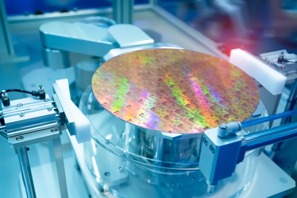
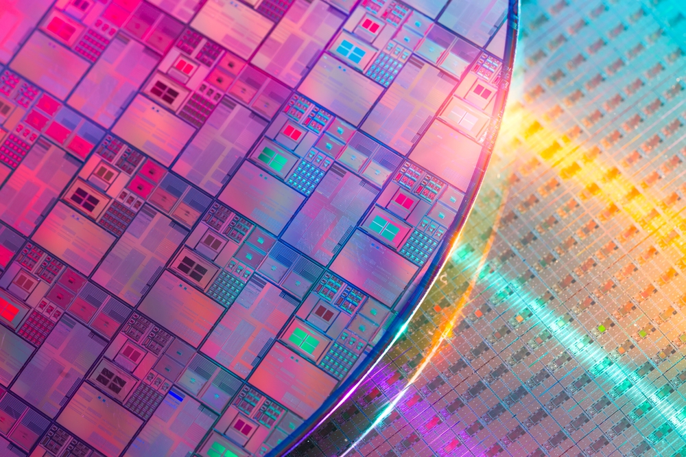
From smartphones to autonomous cars to AI supercomputers, nearly every electronic innovation we use today depends on complicated structures at the atomic scale within silicon chips. As these chips increase in processing power and decrease in size, even the smallest fault can cause massive delays.
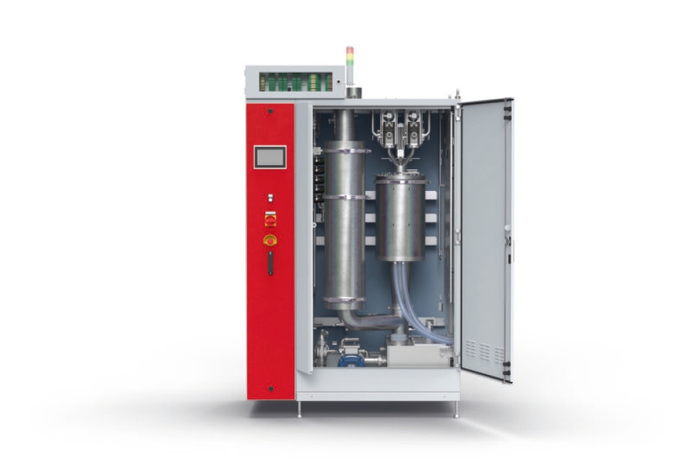
To help chipmakers keep pace and minimize delays, Thermo Fisher Scientific has introduced the Thermo Scientific™ Helios™ MX1 Plasma Focused Ion Beam (PFIB) Scanning Electron Microscope (SEM). This system enables chip manufacturers to visualize and analyze buried semiconductor structures directly within fabrication (fab) environments.
Helios MX1 uses automated 3D reconstruction and metrology to significantly enhance the analysis of semiconductor logic, memory and advanced packaging devices. This fully automated wafer analysis system is uniquely designed to increase productivity in the fab by accelerating time-to-data — the speed at which engineers can see and understand what’s happening deep within a semiconductor.
Seeing the unseen
By integrating high-resolution laboratory instrumentation into the fab environment, Helios MX1 quickly reveals details that were previously only achievable in a lab. This accelerates time-to-yield by providing fast, accurate and valuable insights into semiconductor subsurface defects.
“With Helios MX1, semiconductor fab engineers can now see what was previously only visible in a laboratory,” said Mohan Iyer, semiconductor vice president and general manager at Thermo Fisher Scientific. “The semiconductor industry is witnessing a dramatic increase in the amount of analysis needed within fabrication environments, and traditional methods are no longer sufficient. With Helios MX1, our customers can now have a detailed, three-dimensional look at structures that are beneath the wafer surface.”