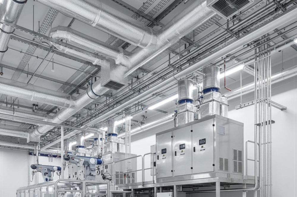
Semiconductor Inspection System market: driving precision and reliability
Market Outlook and Forecast
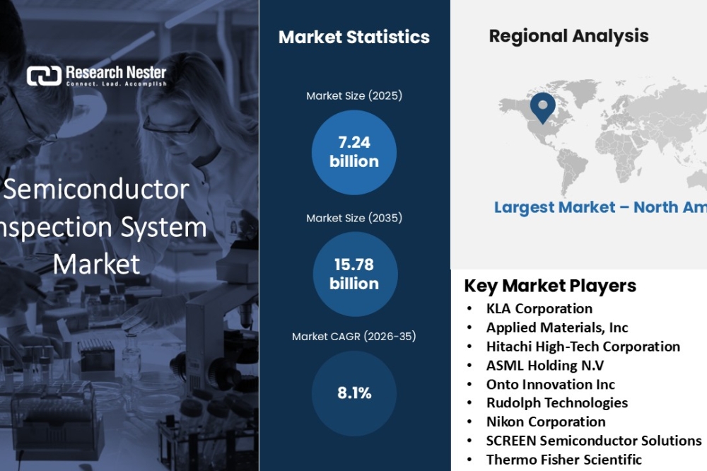
The market, valued at USD 7.24 billion in 2025, is projected to reach USD 15.78 billion by 2035, growing at a steady 8.1% CAGR between 2026 and 2035. As semiconductor fabrication becomes more intricate, inspection systems have become indispensable for ensuring yield enhancement, defect reduction, and process optimization across all manufacturing stages.
Regional Performance Highlights
North America is anticipated to maintain its dominance, accounting for nearly 69.2% of the global revenue share by 2035. The region’s leadership stems from the strong presence of major semiconductor foundries, advanced R&D infrastructure, and government initiatives promoting chip manufacturing independence. The U.S. CHIPS and Science Act, for instance, has spurred massive investments in fabrication facilities and related inspection systems, enabling companies to modernize and expand their manufacturing capabilities.
Europe continues to emerge as a key player, driven by its focus on sustainable electronics manufacturing, automation, and high-end chip design. European semiconductor producers are integrating advanced inspection technologies to meet stringent EU quality and environmental standards, particularly within automotive and industrial electronics sectors.
Meanwhile, the Asia Pacific region is expected to witness the fastest growth through 2035, supported by massive production capabilities in countries such as Taiwan, South Korea, Japan, and China. With the proliferation of consumer electronics, electric vehicles, and IoT devices, demand for wafer and mask inspection systems is surging. Asia’s investments in 3D packaging, AI chips, and miniaturized semiconductors have further accelerated adoption of next-generation inspection systems.
Segment Demand and Use Cases
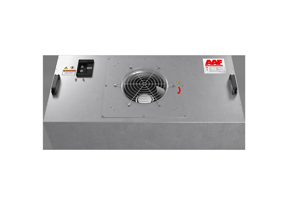
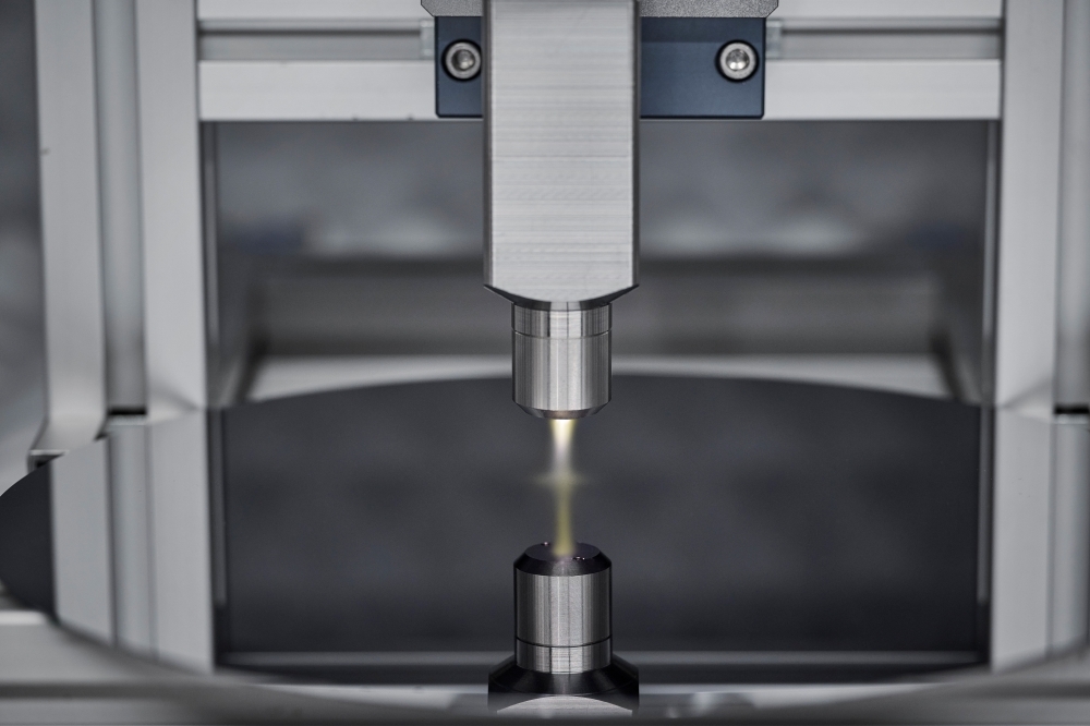
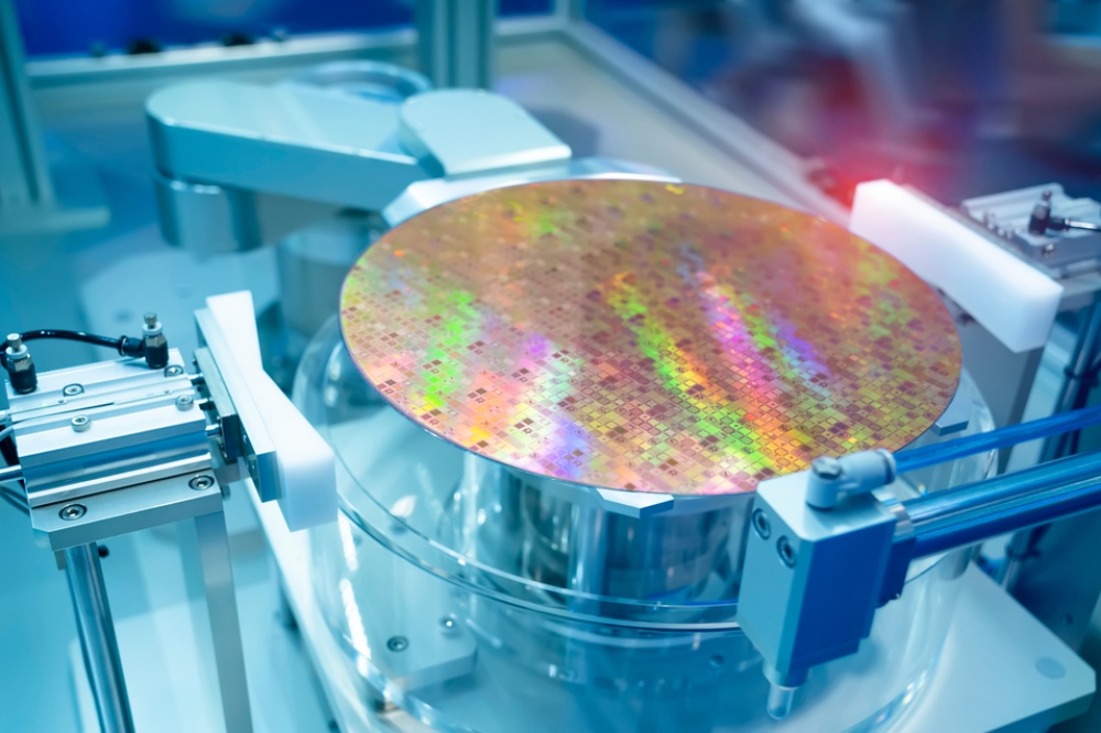
By segment, the wafer inspection segment is expected to register rapid revenue growth during the forecast period. Wafer inspection systems play a critical role in detecting pattern defects, particles, and lithography errors at nanometer scales. As chip geometries continue to shrink, wafer-level inspection technologies such as electron beam inspection and optical metrology are becoming essential for maintaining manufacturing precision.
In terms of end-user segmentation, large enterprises will continue to dominate, accounting for 71% of total revenue by the end of 2035. Large-scale semiconductor manufacturers and foundries have the financial and technical resources to invest in high-end inspection equipment, ensuring process optimization and yield improvement. Smaller fabs, while increasingly exploring AI-based defect detection solutions, are likely to adopt cloud-integrated inspection systems to reduce operational costs and enhance efficiency.
Top Market Trends
1. Integration of AI and Machine Learning in Inspection Processes
Artificial intelligence (AI) and machine learning (ML) are revolutionizing semiconductor inspection systems by enabling real-time defect classification and predictive analytics. Modern inspection systems leverage AI algorithms to automatically distinguish between critical and non-critical defects, reducing false positives and optimizing yield. Companies like KLA Corporation and Applied Materials have introduced AI-powered platforms capable of adaptive learning—allowing inspection tools to improve accuracy over time.
This trend not only increases manufacturing efficiency but also lowers operational costs by minimizing manual review and re-inspection efforts.
2. Rising Demand for Advanced Packaging and 3D IC Inspection
As chipmakers transition from traditional planar designs to 3D integrated circuits (3D ICs) and advanced packaging technologies, inspection complexity has increased significantly. Detecting buried defects and voids within stacked layers requires sophisticated imaging and metrology solutions. To meet these challenges, manufacturers are deploying hybrid inspection systems that combine optical, X-ray, and electron-beam technologies for comprehensive analysis.
This shift has prompted suppliers to develop multi-dimensional inspection solutions capable of analyzing sub-micron features and improving interconnect reliability—essential for next-generation chips used in AI accelerators, autonomous vehicles, and high-performance computing.
3. Growing Emphasis on Sustainability and Energy Efficiency
Sustainability has become a core design consideration in the semiconductor industry. Modern inspection systems are being engineered to consume less energy, optimize maintenance schedules, and reduce waste. Semiconductor fabs are increasingly adopting energy-efficient tools and predictive maintenance solutions to minimize downtime and extend equipment lifespan.
For example, ASML and Hitachi High-Tech have introduced inspection systems that integrate smart power management features and recyclable components, aligning with global ESG and green manufacturing goals. This trend reflects how the semiconductor ecosystem is balancing performance optimization with environmental responsibility.
4. Rising Demand from Emerging Technologies
Emerging applications such as 5G, AI, autonomous vehicles, and IoT devices are placing unprecedented performance demands on chips. These technologies require inspection systems capable of identifying defects at atomic scales and ensuring the reliability of complex circuitry. As a result, demand for high-resolution wafer and mask inspection tools is rising among manufacturers producing advanced logic and memory devices.
The expansion of the EV and renewable energy sectors has also intensified the need for defect-free power semiconductors, further driving market growth.
Recent Company Developments
The competitive landscape of the semiconductor inspection system market is defined by strategic mergers, technological advancements, and significant R&D investments. Leading players are expanding their product portfolios, integrating AI-driven capabilities, and strengthening partnerships with global semiconductor foundries.
1. KLA Corporation
KLA remains a dominant force in the market, continuously enhancing its portfolio of wafer and reticle inspection tools. In 2025, the company introduced a next-generation optical inspection platform featuring machine learning algorithms for improved defect analysis. Its investments in predictive process control and metrology solutions have positioned it as a critical partner to semiconductor foundries worldwide.
2. Applied Materials, Inc.
Applied Materials has advanced its inspection solutions with AI-based platforms designed to handle 3D structures and nanoscale defects. The company’s focus on integrating inspection with process control systems enables semiconductor fabs to optimize yield and throughput. Its collaborations with leading chip manufacturers are strengthening its role in the 3D packaging inspection domain.
3. Hitachi High-Tech Corporation
Hitachi continues to expand its lineup of electron-beam and optical inspection tools. Its newly launched systems provide improved sensitivity for advanced nodes below 5nm. The company’s focus on sustainable inspection technologies and remote diagnostic capabilities has made it a preferred partner for eco-conscious semiconductor fabs.
4. ASML Holding N.V.
Best known for its lithography equipment, ASML has also made significant strides in defect inspection technologies. Through strategic partnerships and in-house R&D, the company is developing integrated inspection systems that align with extreme ultraviolet (EUV) lithography processes, helping chipmakers identify pattern defects during high-resolution imaging.
5. Onto Innovation Inc.
Onto Innovation is leveraging its expertise in metrology and inspection to offer integrated solutions for process optimization. The company’s Dragonfly G3 inspection platform has gained traction in 3D NAND and advanced logic applications, enabling customers to improve yield and device reliability.
6. Rudolph Technologies (part of Onto Innovation)
Rudolph Technologies continues to focus on inspection and metrology tools tailored for advanced packaging applications. Its emphasis on data analytics integration allows fabs to make faster, more informed decisions during defect analysis and process monitoring.
7. Nikon Corporation
Nikon has diversified its semiconductor inspection product portfolio with precision optical metrology systems designed for high-resolution defect detection. The company’s strategic expansion into AI-integrated inspection tools marks its commitment to staying competitive in sub-5nm technologies.
8. SCREEN Semiconductor Solutions
SCREEN is expanding its global presence with high-throughput inspection systems suitable for wafer-level and packaging-level inspection. Its focus on modular, upgradeable platforms allows manufacturers to scale inspection capacity efficiently as production volumes grow.
9. Thermo Fisher Scientific
Thermo Fisher’s advanced electron microscopy and defect characterization tools continue to be vital in semiconductor R&D environments. The company’s acquisition initiatives and AI integration strategies underscore its growing influence in materials analysis for next-generation semiconductor devices.
10. Lasertec Corporation
Lasertec, a pioneer in mask inspection technology, has strengthened its market position with high-resolution EUV mask inspection systems. These tools are instrumental for chipmakers producing cutting-edge semiconductor designs, ensuring defect-free lithography at nanoscale dimensions.
The semiconductor inspection system market stands at the core of the global semiconductor manufacturing ecosystem. As chips become smaller, more powerful, and more complex, the need for precision inspection systems has never been greater. With strong growth prospects across North America, Europe, and Asia Pacific, and technological trends such as AI-driven inspection, 3D packaging analysis, and sustainability integration, the market is set to play a pivotal role in shaping the future of semiconductor production.
From predictive defect analysis to sustainability-driven designs, inspection systems are evolving from quality assurance tools into strategic enablers of innovation, efficiency, and reliability in the digital age.
Source: https://www.researchnester.com/reports/semiconductor-inspection-system-market/7085