Bosch commits €1bn investment to new fab to support IoT strategy

Bosch has announced it will be building a new wafer fab in Dresden, Germany, as part of its commitment to investing in internet of things (IoT) technology.
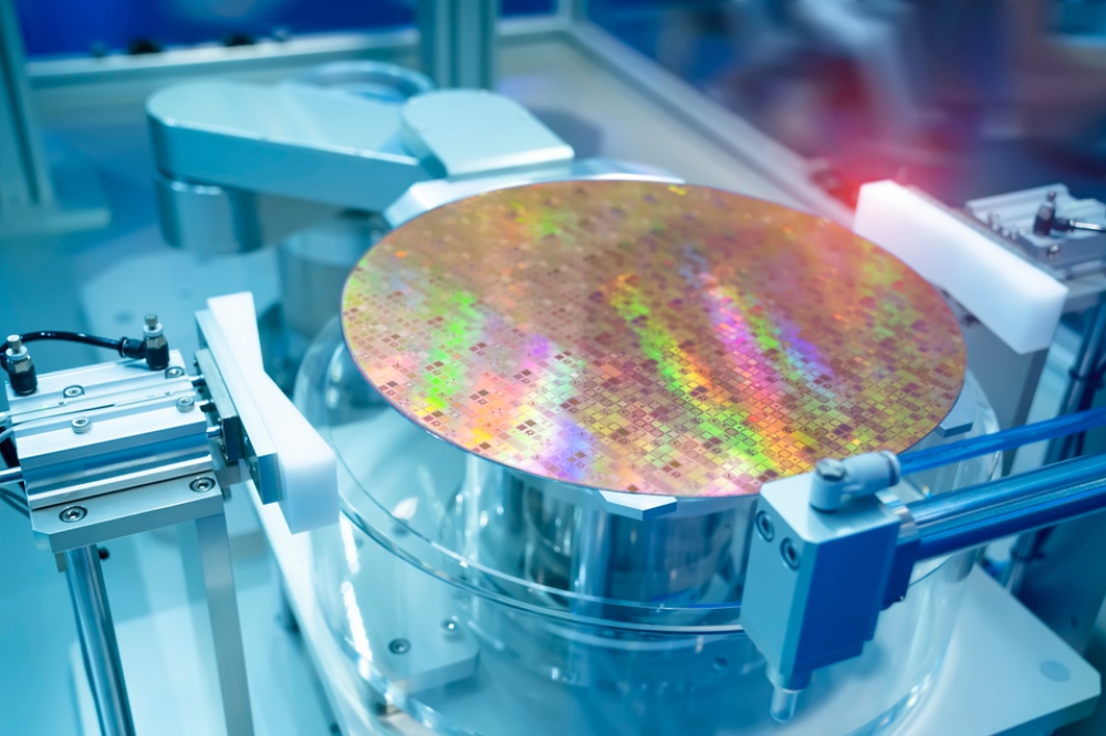
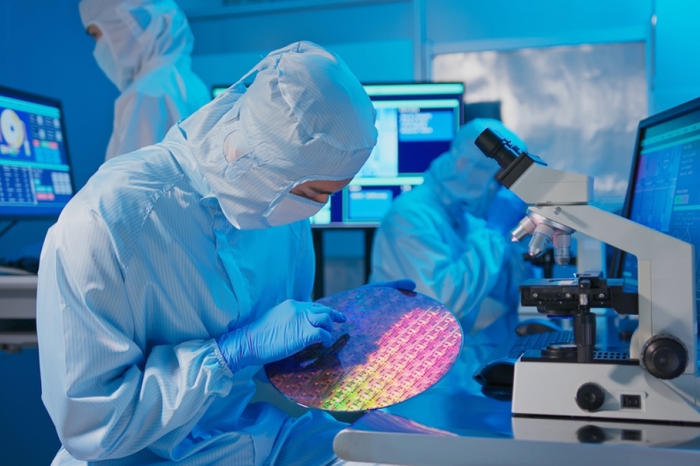
The new location will manufacture the 12-inch wafer chips used in a growing number of IoT and mobility applications. Construction of the high-tech plant is expected to complete by the end of 2019, with manufacturing operations starting towards the end of 2021. Total investment will come to around €1bn, with as many as 700 new jobs created.
Dr. Volkmar Denner, Chairman of the Robert Bosch GmbH Board of Management said: "The new wafer fab is the biggest single investment in Bosch's more than 130-year history. "Semiconductors are the core components of all electronic systems. With connectivity and automation growing, they are being used in more and more areas of application. By extending our semiconductor manufacturing capacity, we are giving ourselves a sound basis for the future and strengthening our competitiveness."
The investment in the new fab marks a key milestone in Bosch's IoT growth strategy. According to a study by PwC, the global semiconductor market is set to grow by more than 5 percent annually up to 2019, with the mobility and IoT market segments growing especially strongly.
12-inch technology as the basis for economies of scale
Semiconductors are an essential technology for the modern age, as they enable manufacturing, mobility and homes to become increasingly connected, electrified, and automated.
Bosch's move into 12-inch wafer technology means it can offer the economies of scale necessary to meet the rising demand for semiconductors triggered by the growth in smart homes and cities.
Leading semiconductor manufacturer and pioneer of MEMS fabrication
With a rich heritage in the manufacture of semiconductors, Bosch has been making several varieties, particularly focussed on application-specific integrated circuits (ASICs), power semiconductors and micro-electro-mechanical systems (MEMS) for more than 45 years.
Bosch is a pioneer and the world's leading manufacturer of MEMS sensors. Over 20 years the company developed the microfabrication technique, known worldwide as the "Bosch process" which is also used to make semiconductors and Bosch ASICs have been used in vehicles since 1970. They are customised to individual applications, and essential for functions such as airbag deployment. In 2016, every car rolling off the production lines worldwide had on average more than nine Bosch chips on board.
At its wafer fab in Reutlingen, Germany, Bosch currently manufactures around 1.5 million ASICs and 4 million MEMS sensors a day. Today, 75 percent of Bosch MEMS sensors are used in consumer and communications electronics applications and can be found in three out of four smartphones. Bosch's current semiconductor portfolio includes acceleration, yaw, mass-flow, pressure, and environmental sensors, as well as microphones, power semiconductors, and ASICs for vehicle ECUs.


