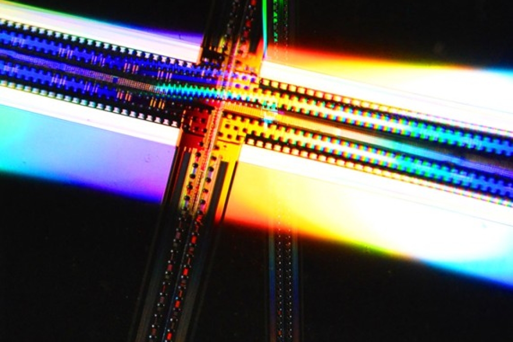
Production system for double-sided wafer probe test for silicon photonics

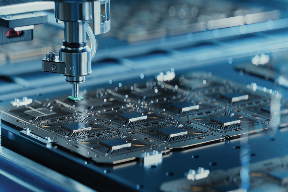
Teradyne has partnered with ficonTEC, a global leader in production solutions for photonics assembly and test, to announce the availability of the first high-volume, double-sided wafer probe test cell for silicon photonics.
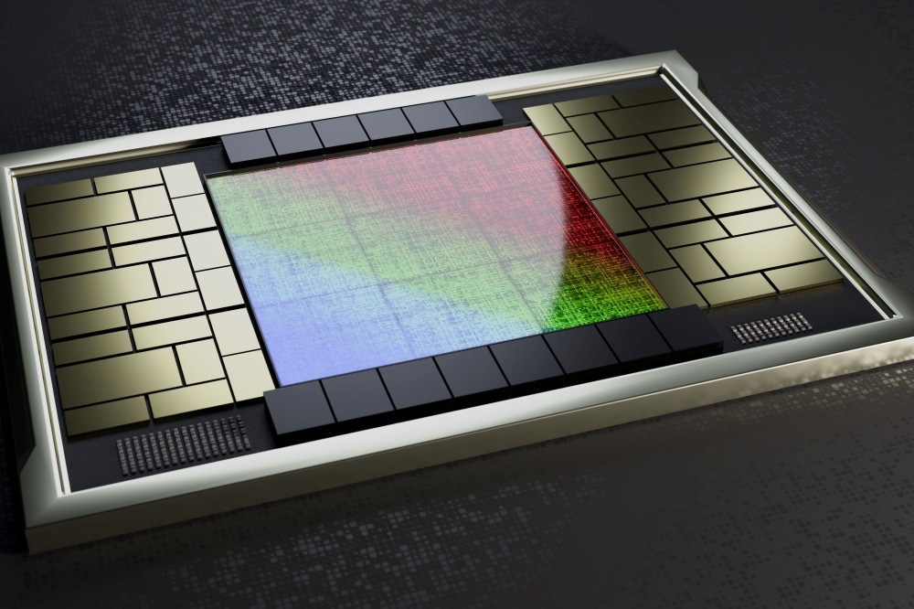
This innovative solution is designed to meet the growing demand for high-throughput electro-optical testing of silicon photonic wafers driven by co-packaged optics (CPO) applications.
The new test cell integrates Teradyne's UltraFLEXplus automated test equipment (ATE) and programming environment, IG-XL, with ficonTEC's advanced optical alignment, probing, and wafer handling technologies. This collaboration enables the testing of hybrid bonded PIC/EIC wafers in a production environment.
While the partnership with ficonTEC enables Teradyne to bring a production-ready system to market today, Teradyne is committed to fostering an open ecosystem for silicon photonics and CPO testing. By ensuring that the UltraFLEXplus is compatible with industry-leading optical instrumentation, probers, alignment systems, and probe cards, Teradyne is delivering a seamless and flexible testing environment for its customers.
"At Teradyne, we believe in the power of collaboration and innovation. Our partnership with ficonTEC enables us to deliver the first high-volume double-sided test cell for silicon photonics wafer test to meet the quickly evolving needs of the industry. Our commitment to an open ecosystem ensures our customers can choose the solution that is right for them," said Regan Mills, President, Product Test at Teradyne.
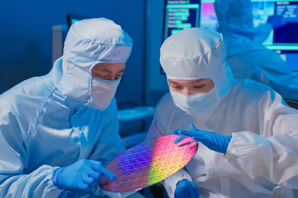
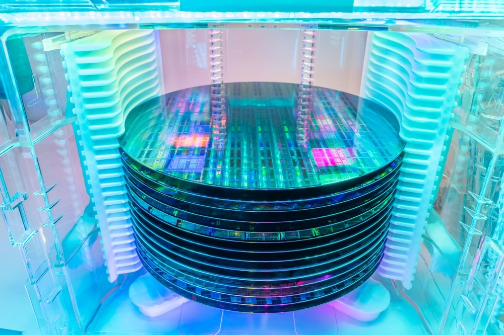
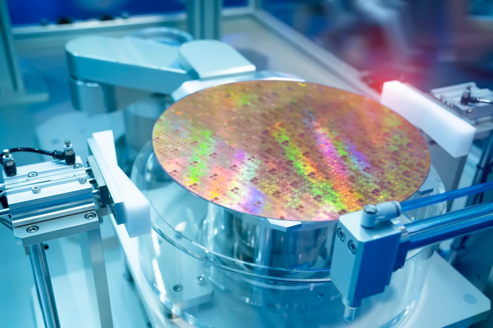
The introduction of the double-sided wafer probe test cell is expected to have a significant impact on the silicon photonics and CPO market. By enabling high-throughput electro-optical testing of silicon photonic wafers, this solution addresses the critical need for known good die testing before wafers are diced and packaged into CPO devices or pluggable transceivers.
The integration of Teradyne's UltraFLEXplus and ficonTEC's optical alignment and probing technologies ensures that the test cell operates efficiently within the existing fab and OSAT test floor infrastructure, providing a comprehensive and cost-effective solution.
"ficonTEC is proud to partner with Teradyne to pioneer this innovative solution for the rapidly developing market. Our joint effort uniquely combines the class-leading capability of both companies, delivering a high-throughput, cost-effective test solution for silicon photonics and CPO manufacturing workflows," said Stefano Concezzi, Corporate Vice President at ficonTEC.