3D Stacking technology advances Embedded AI in Image Sensor development

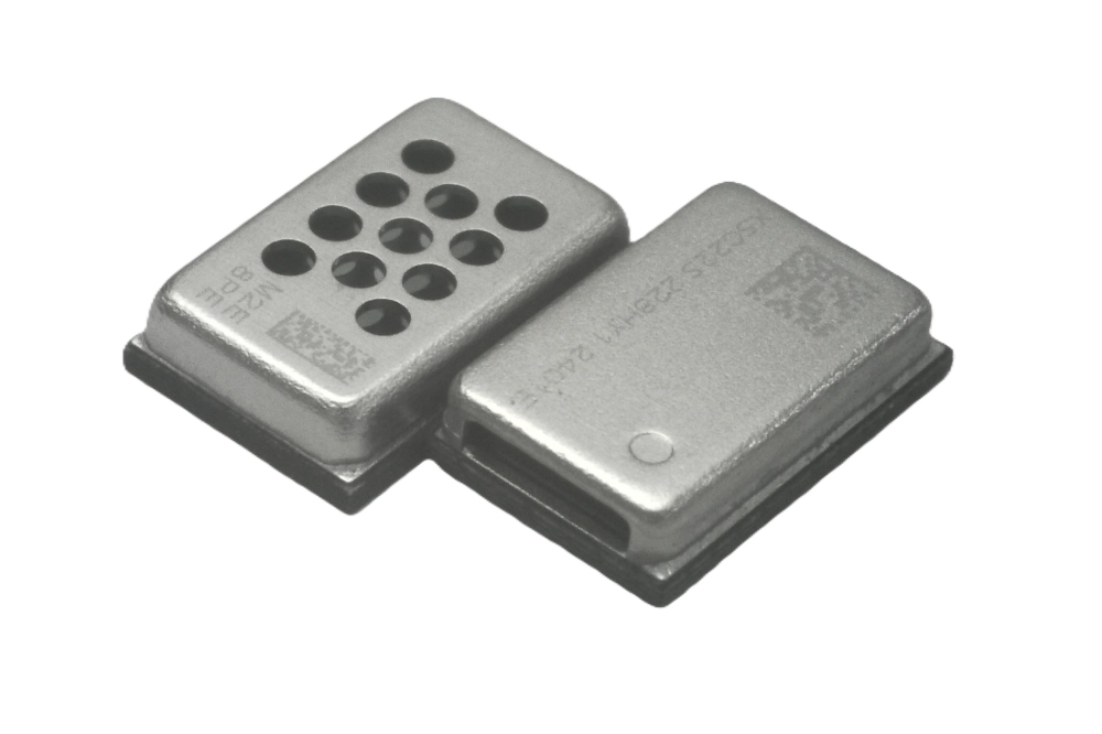
SI Sensors reports progress on designing a next generation image sensor that enables high-speed artificial intelligence (AI) processing within the sensor unit, on top of image processing.
Traditionally image sensor design has primarily focused on capturing high-quality images and transmitting raw data to central processing units for analysis. However, the advent of embedded AI on image sensors offers a transforming way of capturing and processing visual data.
By incorporating AI directly into the sensor, these devices can now perform complex data processing tasks on chip - reducing both latency and power consumption while enhancing performance. In high-speed imaging applications, embedded AI can be used to process data and significantly reduce the output from image sensors. This has been shown to alleviate the transmission bottleneck and enable higher frame rate and dynamic range. By processing most data locally, the necessity to transmit sensitive information externally is minimised. This is especially valuable in fields like health and security, where data protection is paramount.
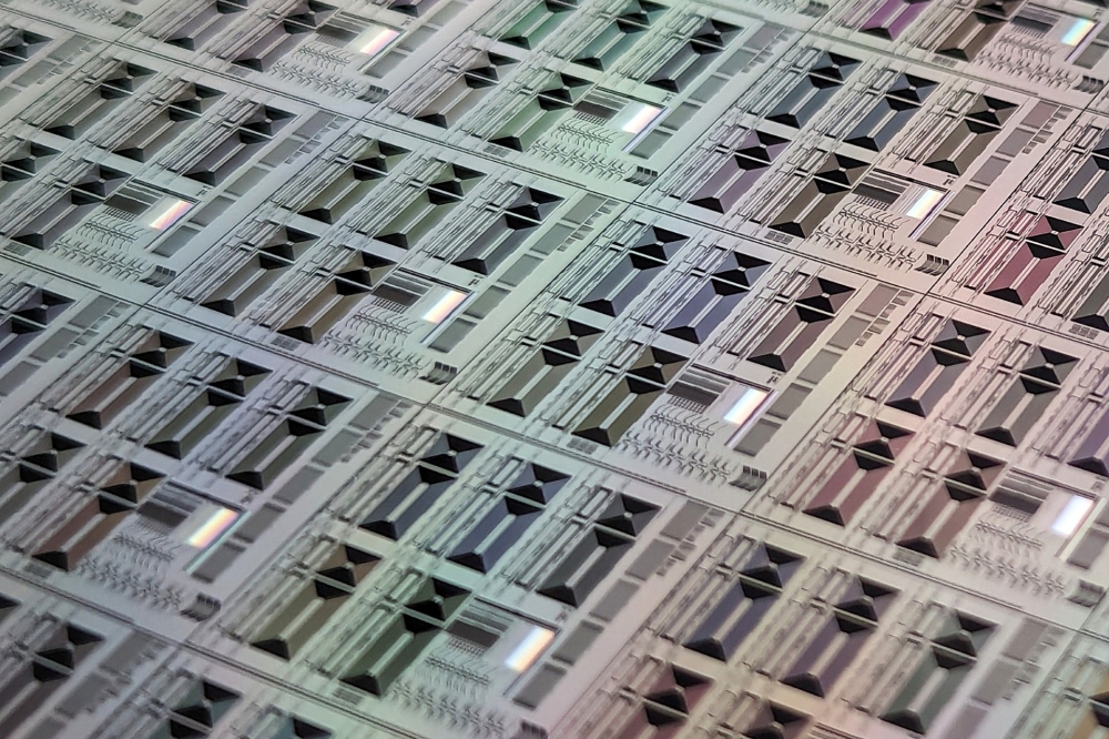
Philip Brown, General Manager of SI Sensors commented “One of the major advances in the development of Embedded AI in Image Sensors is the implementation of 3D stacking technology. This technique allows for the integration of various components, such as Analog-to-Digital converters, memory elements, and signal processing circuits, beneath the image sensor pixel array. By reducing track lengths and increasing density, this approach significantly enhances performance.”
He added “At this stage of our development we are now seeking partners in applications including smart phones, autonomous vehicles, industrial automation, healthcare and high-speed imaging who could benefit from the numerous benefits offered by our embedded AI in image sensor technology.”
SI Sensors are a division of Specialised Imaging, focused on innovative CMOS image sensor design and development. The company’s aim is to use its extensive in-house IP and design experience, together with the latest software tools, to design novel image sensors using the most appropriate foundry technologies globally. The full-service CMOS image sensor design offered by the company includes circuit design, pixel optimisation, simulation, layout, verification, and tape-out. In addition, to ensure performance and consistent quality and reliability SI Sensors perform detailed electro-optical testing from characterisation through to mass production testing adhering to industry standards such as EMVA 1288.

