Collaborative EU Project set to deliver breakthrough in Space Imaging Sensing
Multi-partner efforts will result in development of innovative CMOS sensors that create a competitive advantage for European prime and equipment manufacturers.
A consortium funded by the European Union (EU) is developing advanced high-resolution image sensing technology that could be used in a variety of space missions, including Earth observation, planetary exploration, and scientific research.
The three-year Technology for European iNdependence in Space Image Sensor (TENSIS) project will address the EU-based development of advanced CMOS imaging sensors. The project will aim to create a strategic, competitive advantage for European prime and equipment manufacturers and reduce the dependence on critical technologies and capabilities from outside the EU.
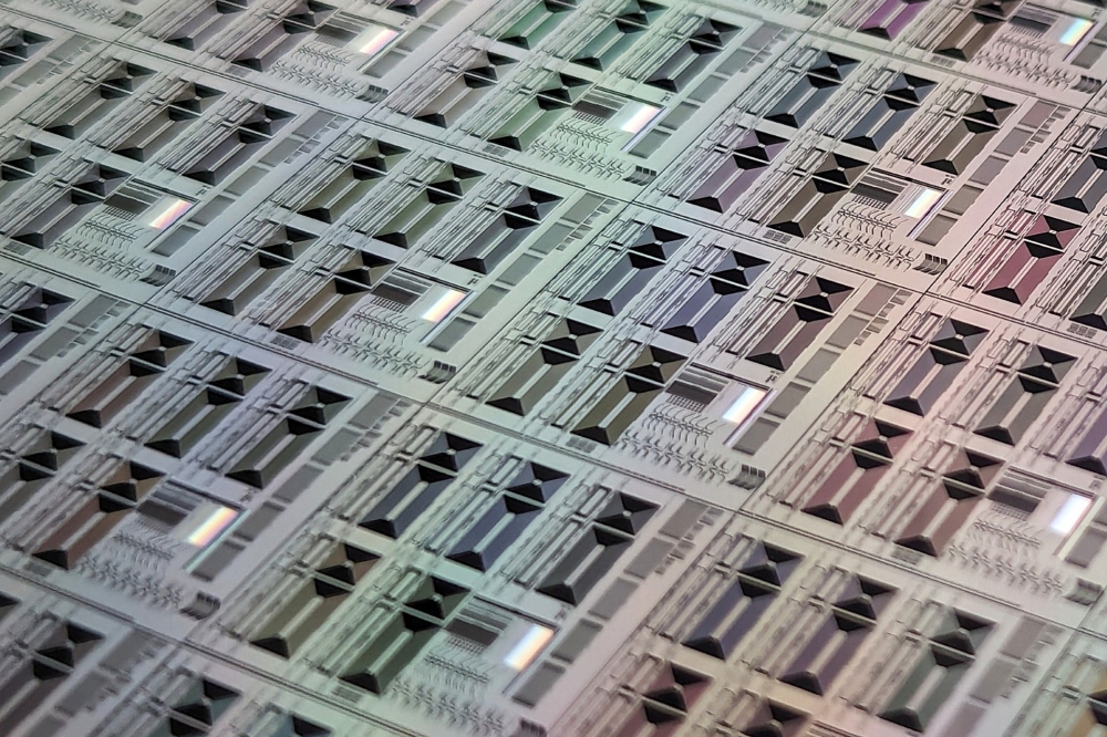
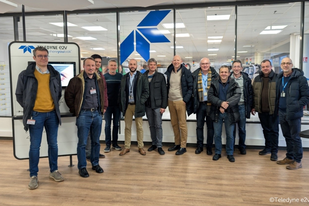
The program was launched on 11 February 2025 at an inauguration event in consortium member Teledyne e2v facilities in Saint-Egrève, Grenoble Area, France. It aims to validate a scalable, large-area, high-resolution, radiation tolerant, customizable, and affordable 180nm CMOS detector, with the key technical characteristics of a 24K x 16K stitched CMOS matrix of 400MPixels. A smaller 4K x 4K stitched CMOS array will also be designed and manufactured.
The project comprises several industrial partners, each of whom brings valuable expertise. Teledyne e2v Semiconductors SAS (France) and Teledyne Innovaciones Microelectronicas SL (Spain) will oversee the project, design the detectors, including the pixel, while imec (Belgium) will manage the development of the optical stack on top of the CMOS detector including filters and optical microlenses.
Meanwhile, Airbus Defence and Space SAS (France) will lead the development of the test equipment and assess the performance of the detector prototypes. Alter Technology Tüv Nord (Spain) will validate the smaller 4K x 4K detector for use in the space environment.
“TENSIS will result in the development of advanced image sensors for space that are high-resolution and durable against space conditions,” says Marc Iliozer, Project & Engineering Director at Teledyne e2v. “The project will help establish strategic capability in Europe and ensure independence in space technology for years to come.”
The project will run until 31 December 2027. The 24k x 16k stitched CMOS array is expected to reach Technology Readiness Level (TRL) 6, with a prototype sensor tested in a relevant environment. The 4k x 4k CMOS detector will reach TRL7, taking it one step closer to final product development.
“The partners are excited to be collaborating on the TENSIS project,” adds Marc. “It is a venture that epitomizes the spirit of European innovation and cooperation.”

