+44 (0)24 7671 8970
More publications     •     Advertise with us     •     Contact us
 
Loading...
News Article

Automated Thickness Measurement System Speeds Production

News


The labor-intensive, manual process of recording precise measurements across various wafer coordinates is now programmable for automated data collection and report generation.

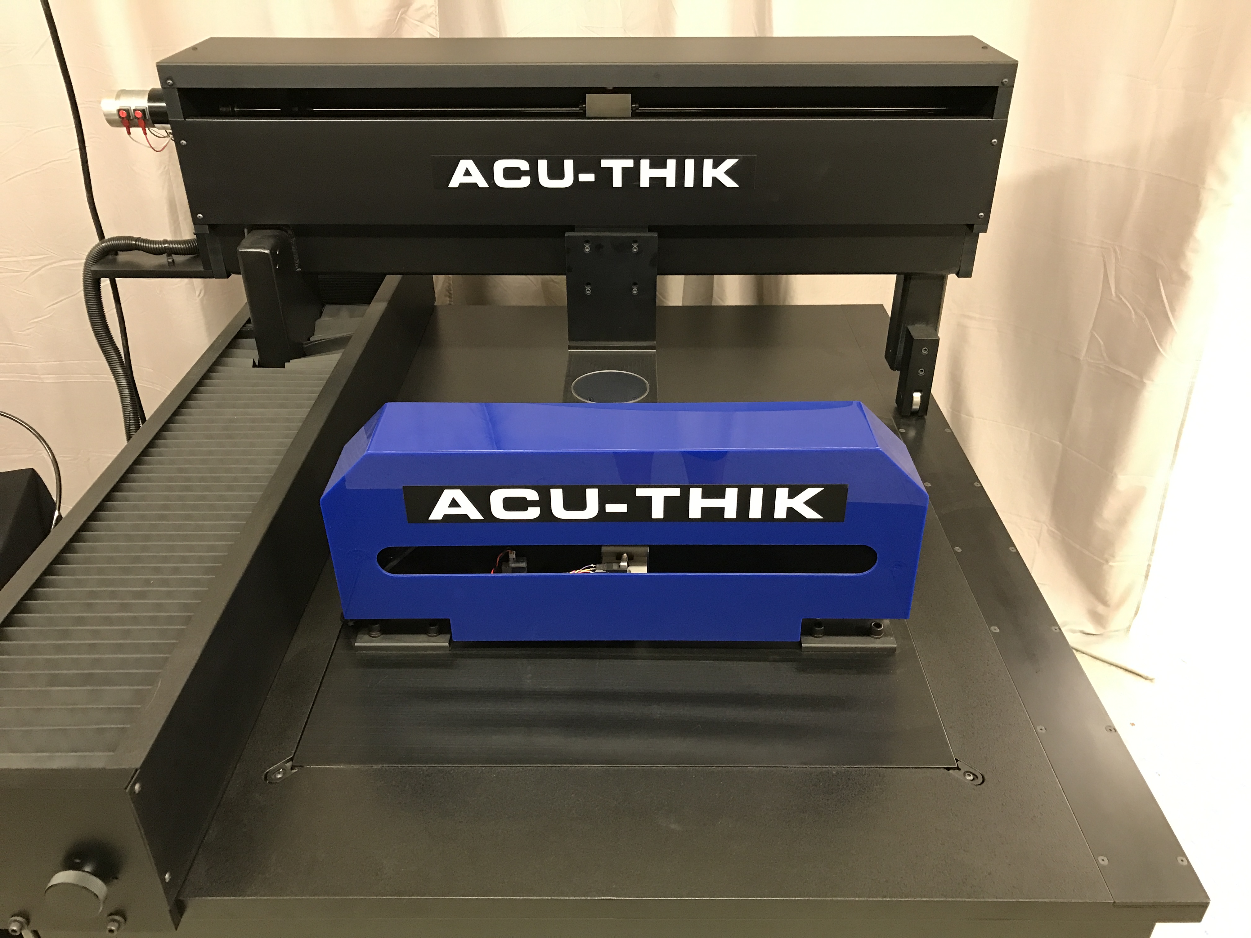
ACU-THIK is an automated thickness measurement tool incorporating dual contact probes for high accuracy inspection of semiconductor wafers. Six Heidenhain measuring devices are integrated into the ACU-THIK system which can be configured to accommodate wafer diameters of 100 mm "“ 400 mm and larger. Acu-Gage customers can have a system customized for their precise needs to make differential gage measurement faster and easier.

Diagnosing as well as controlling thickness, bow and warp in semiconductor wafer production is now automated when using ACU-THIK. Users can preprogram multiple pattern operations to fulfill planned production cycles. Additionally, the system supports robotics integration to further free up operators for other important tasks.

ACU-THIK's automated measurements can improve quality-assured production yields by:
"¢ Calculating wafer thickness across X/Y points to resolution and repeatability of .00025mm/.00001 inch (10 millionths of an inch)
"¢ Determining the amount of bow deviation in an unclamped wafer established by three or more points at equidistant locations

"¢ Examining the entire wafer for warp by incorporating more comprehensive data points to provide a more useful measurement of the full wafer shape

"¢ Accelerating throughput with 15 data points of X/Y thickness measurements in under two minutes as well as increasing accuracy of wafer thickness and flatness definitions

"¢ Validating pre- and post-measurement integrity of data collection for each wafer inspection - ACU-THIK calculates the thickness of a certified gage block prior to as well as after the wafer inspection routine is complete.

The X/Y location for each thickness data point automatically outputs to Excel for further analysis. Programming software runs on Windows 7. Both hardware and software come delivered as a turnkey system including installation and training.

Biden-Harris Administration unveils preliminary terms with GlobalWafers
UK-India Technology Security Initiative launches in New Delhi
Chiplets increase performance and lower cost
Physik Instrumente opens Technology Hub in Southwest Germany
42 Technology partners with INFICON
Imec achieves record-low charge noise for Si MOS quantum dots
Infineon and Amkor sign MoU
Lattice extends Small FPGA portfolio
Nearfield Instruments secures €135 million in funding round
Experts urge EU to increase investment in photonics or risk falling behind China
Reality AI Explorer Tier offers free AI/ML development access
AEM introduces new generation of Automated Burn-In Systems
NPUs are emerging as the main rival to Nvidia’s AI dominance, says DAI Magister
Camtek receives a $20M order from a Tier-1 OSAT
Free samples of every STMicroelectronics NPI IC available from Anglia
NY CREATES and SEMI sign MoU
Major government investment to 'propel' Canada
QuickLogic announces $5.26 million contract award
ASNA and Athinia collaborate
Global sales forecast to reach record $109 billion in 2024
AMD to acquire Silo AI
Nanotronics unveils 'groundbreaking' Gen V AI Model
Aitomatic unveils SemiKong
Biden-Harris Administration reveals first CHIPS for America R&D facilities and selection processes
Collaboration to produce cutting-edge AI accelerator chips
Oxford Ionics breaks global quantum performance records
Adeia wins ECTC Award for paper on “Fine Pitch Die-to-Wafer Hybrid Bonding”
AEM introduces new generation of Automated Burn-In Systems
Sydney council forges vital semiconductor agreement
EV Group's EVG880 LayerRelease wins 2024 Best of West
Biden-Harris Administration to invest up to $1.6 billion
Cyient sets up subsidiary for semiconductor business
×
Search the news archive

To close this popup you can press escape or click the close icon.
Logo
×
  • 1st January 1970
  • 1st January 1970
  • 1st January 1970
  • 1st January 1970
  • 1st January 1970
  • 1st January 1970
  • 1st January 1970
  • 1st January 1970
  • View all news 22645 more articles
Logo
×
Register - Step 1

You may choose to subscribe to the Silicon Semiconductor Magazine, the Silicon Semiconductor Newsletter, or both. You may also request additional information if required, before submitting your application.


Please subscribe me to:


You chose the industry type of "Other"

Please enter the industry that you work in: