
Wafer bonding solutions for heterogeneous integration and wafer-level packaging
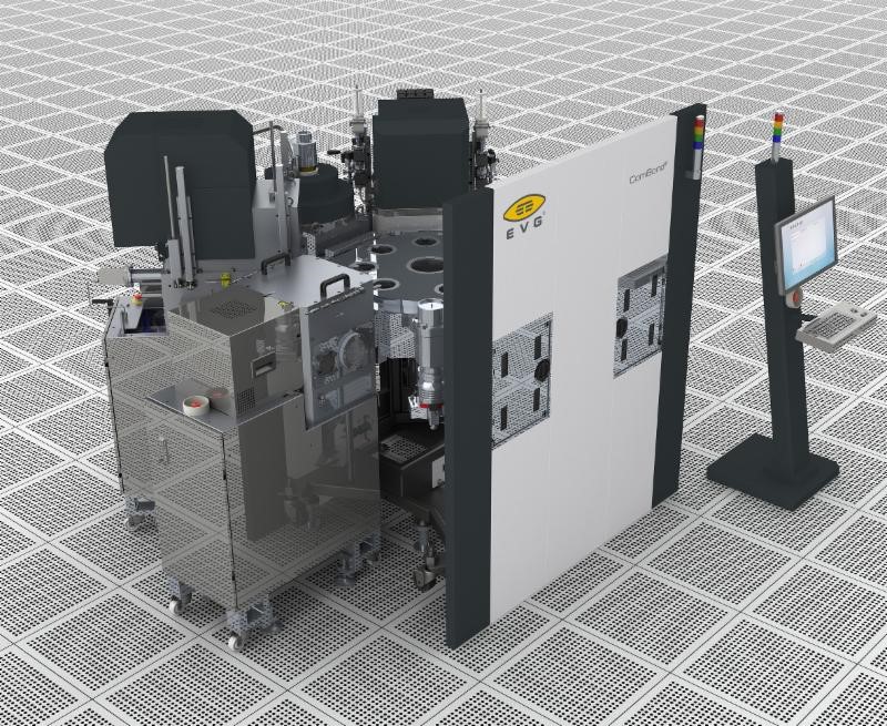
EVG ComBond® automated high-vacuum wafer bonding system
EV Group (EVG), a supplier of wafer bonding and lithography equipment for the MEMS, nanotechnology and semiconductor markets, has announced that new developments in heterogeneous integration and wafer-level packaging enabled by its advanced wafer bonding solutions will be highlighted in several papers being presented at the 2019 IEEE 69th Electronic Components and Technology Conference (ECTC), to be held May 28-31 in Las Vegas.
"Optimization of a BEOL Aluminum Deposition Process Enabling Wafer Level Al-Al Thermo-Compression Bonding" (Session 5 - Wednesday, May 29, 10:25am)
This joint paper by EVG, IHP - Innovations for High Performance Microelectronics, and Sabanci University, describes a wafer-level aluminum-aluminum (Al-Al) thermo-compression bonding process used in combination with an optimized Al sputter-deposition process. Surface treatment and subsequent bonding are both performed in a high vacuum cluster via the EVG ComBond® automated high-vacuum bonding system, which provides oxide-free direct bonding of "anything on anything".
• "Al-Al Direct Bonding with Sub-μm Alignment Accuracy for Millimeter Wave SiGe BiCMOS Wafer Level Packaging and Heterogeneous Integration" (Session 20 - Thursday, May 30, 4:45pm)
This joint paper by EVG, IHP - Innovations for High Performance Microelectronics, and Sabanci University, examines the use of the EVG ComBond system to enable Al-Al direct bonding with high alignment accuracy and reduced process temperatures to enable low-cost, fine-pitch wafer-to-wafer interconnections supporting high-performance mm-wave SiGe BiCMOS wafer-level packaging.
• "Ultra-thin QFN-Like 3D Package with 3D Integrated Passive Devices"
(Interactive Poster Session - Wednesday, May 29, 9:00 - 11:00am and 2:00 - 4:00pm)
This interactive joint poster paper by EVG, 3DiS Technologies, Besi, and NXP Semiconductors, describes the development of a novel ultra-thin, substrate-less package that integrates ultra-thin 3D stacked dies and compact 3D inductive devices inside. The work involves the use of EVG's laser debonding solution, which combines a solid-state UV laser and proprietary beam-shaping optics to enable optimized, force-free debonding.
EVG's wafer bonding, lithography and metrology solutions enable the development and high-volume manufacturing of technology innovations in advanced packaging -- including backside illuminated CMOS image sensors and other 3D-IC stacked devices -- as well as in MEMS and compound semiconductors, such as silicon photonics and engineered substrates. Recent breakthroughs in laser debonding for Fan-out Wafer Level Packaging (FO-WLP), wafer bond alignment technology to address future 3D-IC packaging requirements, fusion bonding for front-end-of-line layer transfer processes, and nanoimprint lithography (NIL) to support wafer-level optics (WLO) manufacturing, are just a few examples of EVG's technology leadership in heterogeneous integration and wafer-level packaging.
ECTC attendees interested in learning more about EVG and its suite of wafer bonding, lithography and metrology solutions for heterogeneous integration and wafer-level packaging are invited to visit EVG at booth #409 on May 28-31 at The Cosmopolitan of Las Vegas.


