+44 (0)24 7671 8970
More publications     •     Advertise with us     •     Contact us
 
Loading...
News Article

k-Space Offers a New Accessory for Their In situ Metrology Tools

News

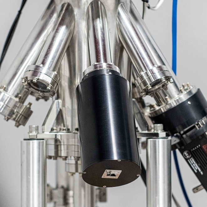
The image shows protective cover in place as the system would be used in a research or production environment

k-Space is proud to announce the addition of a new accessory, kSA Insight, for their metrology tools. This tool allows researchers and operators to view their wafers and platen in real-time from within the k-Space software. The imaging system utilizes a high-resolution color camera and is plug-and play compatible with all k-Space thin-film metrology software.

k-Space CEO, Darryl Barlett, stated “Several customers have requested the ability to see their wafers and platen from their computer screen during deposition, so we designed this tool to seamlessly integrate with their existing k-Space software. So, whether you are running kSA 400, kSA BandiT, kSA MOS, or kSA ICE, you can seamlessly view your platen and wafers with this plug in.”

Customers can adapt the accessory to viewports of various sizes, and the included zoom lens allows for focus over a large range of working distances. The live video can be zoomed in or out, and full resolution color images can be snapped and stored at any time from within the k-Space software.

Laser focus on Glasgow
Kaman Measuring introduces ThreadChecker
SandBox Semiconductor adds hybrid metrology capabilities
Intel empowers developers to 'Bring AI Everywhere'
Fab renovation: A blue CHIPS investment
Aqua Membranes collaborates with Micron Technology
Brewer Science releases Impact Report 2023
UK semiconductor strategy: A patent attorney’s perspective
Wafer cleaning market to reach US$ 17.2 billion
Solvay signs partnership agreement with Shengjian
ACM cleaning platform targets chiplets industry
Vietnam's thriving semiconductor industry fuels economic resilience
GSA celebrates women's innovation
The need for geofencing to help improve semiconductor IP security
All roads lead to Arizona
Time to celebrate and accelerate diversity, equity and inclusion
Cadence completes acquisition of PHY IP assets from Rambus
Wales joins the European Semiconductor Regional Alliance
Magnachip targets EV market
Greene Tweed: When it can’t fail
Advanced Packaging market Size to reach $66.9 billion by 2032
Inventec and Renesas to develop PoC for automotive gateways
Renesas commences Sequans tender offer
Tower Semiconductor and InnoLight partner
Flanders Semiconductors - a new hub in the heart of Europe
Ambiq wins Demo of the Year Award
Advanced packaging market nears US$90 billion
Intel Foundry Services and Tower Semiconductor reach US foundry agreement
MediaTek develops first chip using TSMC's 3nm Process
Advanced X-ray technology for advanced packaging
New developments in underlayers and their role in advancing EUV lithography
Advanced SAM validates integrity of electrostatic chucks
×
Search the news archive

To close this popup you can press escape or click the close icon.
Logo
×
Logo
×
Register - Step 1

You may choose to subscribe to the Silicon Semiconductor Magazine, the Silicon Semiconductor Newsletter, or both. You may also request additional information if required, before submitting your application.


Please subscribe me to:


You chose the industry type of "Other"

Please enter the industry that you work in: