
Virtual fab provides sustainable choices
Imec’s virtual fab underpins strategies to reduce the carbon footprint of lithography and etch process steps.
At the recent 2023 Advanced Lithography + Patterning Conference, imec presented a quantitative assessment of the environmental impact of patterning in advanced IC manufacturing. A virtual fab has been developed in the imec.netzero modeling platform. The resulting analysis enables imec and its partners to assess current manufacturing choices, identify areas of focus, and project the future. In imec’s physical fab, environmentally friendly process solutions are explored for the high impact areas, which include the reduction of fluorinated etch gases, maximizing EUV scanner throughput, and reducing hydrogen and water consumption.
CO2 emissions associated with IC manufacturing are expected to quadruple in the next decade, due to both the increasing complexity of advanced technologies and the projected growth of the total volume of wafers produced. To counter this scenario, leading semiconductor players have committed to becoming carbon neutral or net-zero by 2030-2050. In that context, imec launched its sustainable semiconductor technologies and system (SSTS) program, gathering the supply chain to jointly target net-zero emissions for chip manufacturing. One of the goals of SSTS is to offer the industry a unique bottom-up approach that provides actionable data with a high granularity enabling impact assessment during process and flow development.
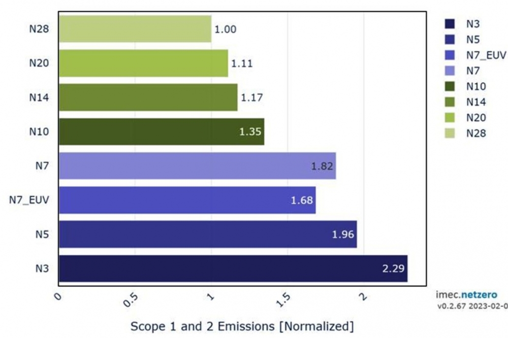
By using imec.netzero, a modeling platform developed in the frame of the SSTS program, imec, in collaboration with its partners, has for the first time quantified the environmental impact of patterning-related process steps for various logic technology nodes. “By applying this ‘virtual fab’ tool, we demonstrated that lithography and etch together are responsible for 45 percent of the Scope 1 and Scope 2 emissions (i.e., emissions from owned or operated assets, and from purchased energy, respectively) associated with fabricating 3nm logic wafers. “The comparison of an advanced technology node (N7 in our sample chart) with and without EUV patterning also clearly demonstrated the value of EUV as a solution to limit the CO2eq emissions associated with complex multi-patterning techniques (10nm-7nm-5nm transition),”explains Emily Gallagher, a principal member of the technical staff at imec. “In addition, the modeling tool can quantify the gains associated with real fab experiments. For example, lowering the EUV dose by ten percent saves about 0.4 kg CO2eq per wafer. This would result in saving about 40 tons of CO2eq per month in a large fab, equivalent to emissions associated with 100 round trip flights from San Francisco, CA to Portland, Oregon.”
Imec uses its physical fab as a pilot environment to explore process and design directions for the high-impact areas. Emily Gallagher: “In collaboration with our partner Edwards, we recently installed a hydrogen recovery system for EUV lithography in our 300mm cleanroom, enabling us to reuse and recover ~ 70 percent of the hydrogen. Additionally, we are increasing focus on low-dose solutions for both 0.33NA and 0.55NA (High NA) EUV lithography, an effort that is also known to reduce costs in lithography. We also identified etch directions for improved sustainability, currently focusing on overall reduction of conventional gas consumption. In a next step, we will, together with our partners, quantify the impact of these proposed solutions in full semiconductor process flows.”
Steven Scheer, senior vice president of advanced patterning, process and materials at imec: “The patterning process steps developed in the past have largely contributed to the semiconductor revolution and further advancements are essential to keep pace with the demand for ever-increasing compute performance. Defining strategies to reduce CO2 emissions while keeping the same patterning capabilities will be a huge effort, for which we have now reached a first milestone. The models developed within imec.netzero are continually benchmarked and validated through partnerships with equipment and material suppliers. Their role will be critical in moving forward with our SSTS initiative and in fostering practical solutions for patterning to reduce the carbon footprint and environmental impact of the global semiconductor industry.”
“We are however mindful that not all environmental impact is captured in the carbon equivalent emission metric,” adds Steven Scheer. “For example, gas emissions can be hazardous air pollutants (HAPS), and both photoresists and antireflection coatings (ARCs) can contain PFAS (per- and polyfluoroalkyl substances). The carbon-fluorine bond strength of PFAS has contributed to the superior performance characteristics of chemically amplified resists (CARs) for both mature optical and evolving EUV photoresists. However, its bioaccumulation potential has led to a strong societal interest to eliminate their use. Projects like PFAS elimination must be considered in addition to those that lower carbon emissions directly.”


