
EVG highlights innovations at ECTC 2023
Papers to highlight breakthrough capabilities of EVG’s hybrid bonding, LITHOSCALE® maskless lithography and NanoCleave™ layer release technology for advanced packaging applications.
EV Group (EVG), a leading supplier of wafer bonding and lithography equipment for the MEMS, nanotechnology and semiconductor markets, has announced that new developments in heterogeneous integration enabled by its advanced wafer-to-wafer (W2W) and die-to-wafer (D2W) bonding, lithography, and revolutionary infrared (IR) laser cleave solutions will be highlighted in multiple papers being presented at the 2023 IEEE 73rd Electronic Components and Technology Conference (ECTC), to be held May 30-June 2 in Orlando, Fla.
* “Aggressive Pitch Scaling (Sub-0.5 μm) of W2W Hybrid Bonding Through Novel Materials and Process Innovations” (Session 1, Heterogeneous Chiplet Integration – Wed., May 31, 10:10am)
Advanced 3D integration nodes face significant challenges in process control and material limitations. Using advanced 300-mm toolsets and process innovations, Applied Materials and EVG study the importance of layout design, bonding dielectric, copper CMP recess control, and bonding overlay control to produce a high-quality bond interface at sub-500-nm pitches.
* “Direct Die to Wafer Cu Hybrid Bonding for Volume Production” (Session 3, Advancements in Copper/Silicon-Oxide Hybrid Bonding – Wed., May 31, 10:10am)
In this joint-paper, ASM Pacific Technology (ASMPT) and EVG demonstrate a complete process for direct D2W hybrid bonding, including die cleaning, surface activation, high-precision D2W die bonding and annealing. High-volume-manufacturing equipment is used in critical processes such as die preparation and die bonding.
* “0.5 μm Pitch Wafer-to-Wafer Hybrid Bonding With SiCN Bonding Interface for Advanced Memory” (Session 27, Next Generation Wafer-to-Wafer Copper Bonding – Fri., June 2, 10:10am)
W2W hybrid bonding enables high vertical interconnect density through small bond pad CD, tight pitch, and high percentage of copper areal density. This joint-paper by Applied Materials and EVG showcases a robust integration flow for W2W hybrid bonding with a silicon carbon nitride (SiCN) interface at 0.5-micron tight pitch bonding across various test patterns on 300-mm wafers.
* “Exploring Capabilities of Maskless Lithography for Dual Image Exposure in FOWLP” (Session 28: Process Enhancements in 3D, FOWLP, and TSV Technologies – Fri., June 2, 9:50am)
In this joint-paper by HD MicroSystems™ and EVG, dual-image patterning of positive tone dielectric material PBO from HD MicroSystems was investigated using EVG’s LITHOSCALE® maskless exposure (MLE) technology, enabling simultaneous pattering of RDL traces and vias in one lithographic step without intermediate alignment.
* “A Study of SiCN Wafer-to-Wafer Bonding and Impact of Wafer Warpage” (Session 34: Bonding Assembly - Novel Packaging, Process, and Characterization – Fri., June 2, 4:05pm)
In this joint-paper by imec and EVG, W2W bonding studies were carried out on blanket and patterned highly warped wafers using SiCN as the bonding dielectric material to gain a deeper understanding of SiCN-to-SiCN direct bonding and to assess the impact of wafer shape on bonding overlay results.
* “Novel IR Laser Cleaving for Ultra-Thin Layer Transfer and 3D Stacked Devices” (Session 38: Interactive Presentations 2 – Wed., May 31, 2:30-4:30pm)
EVG demonstrates how its revolutionary NanoCleave™ IR laser release technology in combination with fusion and hybrid bonding enables 3D integration and full-area wafer stacking. Highlighted use cases include 3D system on chip with multiple stacked memory layers such as SRAM, and 3D integration transferring thin silicon layers for integration processes such as 3D sequential integration. The use of inorganic IR release layers enables nanometer-precision separation of layers and higher processing temperatures, thereby supporting front-end processing and enabling die and wafer processing with thicknesses below 150 nm for improved PPAC.
Special Panel Session
Dr. Thomas Uhrmann of EVG will also participate in a special session panel, “Copper Hybrid Bond Interconnections for Chip-to-Wafer Applications,” moderated by Jan Vardaman of TechSearch International, on Tue., May 30, 10:30am-12:00pm.
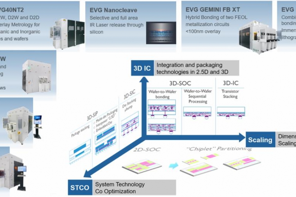
EVG Heterogeneous Integration Solutions
EVG’s wafer bonding, lithography and metrology solutions enable the development and high-volume manufacturing of technology innovations in advanced packaging—including backside illuminated CMOS image sensors and other 3D-IC stacked devices—as well as in MEMS and compound semiconductors. Recent breakthroughs in hybrid bonding to address the needs for 3D device integration, wafer bond alignment technology to address future 3D-IC packaging requirements, IR laser release technology to eliminate glass substrates for advanced packaging and enable thin-layer 3D stacking, maskless exposure for Fan-out wafer level packaging (FOWLP), and nanoimprint lithography (NIL) to support wafer-level optics (WLO) manufacturing, are just a few examples of EVG’s technology leadership in heterogeneous integration and wafer-level packaging.
EV Group’s SmartView® NT3 aligner, available on the company’s GEMINI® FB XT integrated fusion bonding system, provides sub-50-nm wafer-to-wafer alignment accuracy to meet the most aggressive 3D-IC packaging roadmaps.
EVG also engages with companies and research groups across the technology supply chain to develop high-volume manufacturing solutions that drive new innovations in semiconductors, sensors and photonics for a wide variety of automotive, medical, industrial and home entertainment applications.
See EVG at ECTC
ECTC attendees interested in learning more about EVG and its suite of wafer bonding, lithography and metrology solutions for heterogeneous integration are invited to visit EVG at Booth 330 on May 30-June 2 at The Grande Lakes Resort in Orlando, Fla.


