+44 (0)24 7671 8970
More publications     •     Advertise with us     •     Contact us
 
Loading...
News Article

Graphene looks promising as a flexible, low-cost touchscreen solution

New research suggests that graphene-treated nanowires could soon replace current touchscreen technology, significantly reducing production costs and allowing for more affordable, flexible displays

New research published in the journal Advanced Functional Materials suggests that graphene-treated nanowires could soon replace current touchscreen technology, significantly reducing production costs and allowing for more affordable, flexible displays.

The majority of today's touchscreen devices, such as tablets and smartphones are made using indium tin oxide (ITO) which is both expensive and inflexible. Researchers from the University of Surrey and AMBER, the materials science centre based at Trinity College Dublin have now demonstrated how graphene-treated nanowires can be used to produce flexible touchscreens at a fraction of the current cost.

Using a simple, scalable and inexpensive method the researchers produced hybrid electrodes, the building blocks of touchscreen technology, from silver nanowires and graphene.

Dr Alan Dalton from the University of Surrey said, "The growing market in devices such as wearable technology and bendable smart displays poses a challenge to manufacturers. They want to offer consumers flexible, touchscreen technology but at an affordable and realistic price. At the moment, this market is severely limited in the materials to hand, which are both very expensive to make and designed for rigid, flat devices."

Lead author, Dr Izabela Jurewicz from the University of Surrey commented, "Our work has cut the amount of expensive nanowires required to build such touchscreens by more than fifty times as well as simplifying the production process. We achieved this using graphene, a material that can conduct electricity and interpret touch commands whilst still being transparent."

Co-author, Professor Jonathan Coleman, AMBER, added, "This is a real alternative to ITO displays and could replace existing touchscreen technologies in electronic devices. Even though this material is cheaper and easier to produce, it does not compromise on performance."

"We are currently working with industrial partners to implement this research into future devices and it is clear that the benefits will soon be felt by manufacturers and consumers alike."

The research benefited from funding and collaboration with M-SOLV, a touchscreen manufacturer.

Biden-Harris Administration unveils preliminary terms with GlobalWafers
UK-India Technology Security Initiative launches in New Delhi
Chiplets increase performance and lower cost
Physik Instrumente opens Technology Hub in Southwest Germany
42 Technology partners with INFICON
Imec achieves record-low charge noise for Si MOS quantum dots
Infineon and Amkor sign MoU
Lattice extends Small FPGA portfolio
Nearfield Instruments secures €135 million in funding round
Experts urge EU to increase investment in photonics or risk falling behind China
Reality AI Explorer Tier offers free AI/ML development access
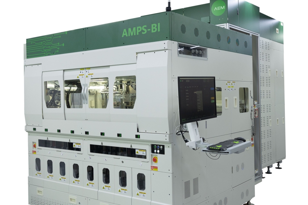
AEM introduces new generation of Automated Burn-In Systems
NPUs are emerging as the main rival to Nvidia’s AI dominance, says DAI Magister
Camtek receives a $20M order from a Tier-1 OSAT
Free samples of every STMicroelectronics NPI IC available from Anglia
NY CREATES and SEMI sign MoU
Major government investment to 'propel' Canada
QuickLogic announces $5.26 million contract award
ASNA and Athinia collaborate
Global sales forecast to reach record $109 billion in 2024
AMD to acquire Silo AI
Nanotronics unveils 'groundbreaking' Gen V AI Model
Aitomatic unveils SemiKong
Biden-Harris Administration reveals first CHIPS for America R&D facilities and selection processes
Collaboration to produce cutting-edge AI accelerator chips
Oxford Ionics breaks global quantum performance records
Adeia wins ECTC Award for paper on “Fine Pitch Die-to-Wafer Hybrid Bonding”
AEM introduces new generation of Automated Burn-In Systems
Sydney council forges vital semiconductor agreement
EV Group's EVG880 LayerRelease wins 2024 Best of West
Biden-Harris Administration to invest up to $1.6 billion
Cyient sets up subsidiary for semiconductor business
×
Search the news archive

To close this popup you can press escape or click the close icon.
Logo
×
  • 1st January 1970
  • 1st January 1970
  • 1st January 1970
  • 1st January 1970
  • 1st January 1970
  • 1st January 1970
  • 1st January 1970
  • 1st January 1970
  • View all news 22645 more articles
Logo
×
Register - Step 1

You may choose to subscribe to the Silicon Semiconductor Magazine, the Silicon Semiconductor Newsletter, or both. You may also request additional information if required, before submitting your application.


Please subscribe me to:


You chose the industry type of "Other"

Please enter the industry that you work in: