
New dimension for integrated circuits: 3-D nanomagnetic logic
Electrical engineers at the Technische Universität Muenchen (TUM) have demonstrated a new kind of building block for digital integrated circuits. Their experiments show that future computer chips could be based on three-dimensional arrangements of nanometer-scale magnets instead of transistors. As the main enabling technology of the semiconductor industry -- CMOS fabrication of silicon chips -- approaches fundamental limits, the TUM researchers and collaborators at the University of Notre Dame are exploring "magnetic computing" as an alternative. They report their latest results in the journal Nanotechnology.
In a 3D stack of nanomagnets, the researchers have implemented a so-called majority logic gate, which could serve as a programmable switch in a digital circuit. They explain the underlying principle with a simple illustration: Think of the way ordinary bar magnets behave when you bring them near each other, with opposite poles attracting and like poles repelling each other. Now imagine bringing several bar magnets together and holding all but one in a fixed position. Their magnetic fields can be thought of as being coupled into one, and the "north-south" polarity of the magnet that is free to flip will be determined by the orientation of the majority of fixed magnets.
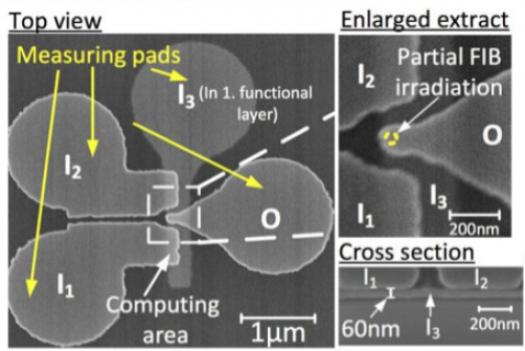
Gates made from field-coupled nanomagnets work in an analogous way, with the reversal of polarity representing a switch between Boolean logic states, the binary digits 1 and 0. In the 3D majority gate reported by the TUM-Notre Dame team, the state of the device is determined by three input magnets, one of which sits 60 nanometers below the other two, and is read out by a single output magnet.
The Latest in a Line of Advances
This work builds on capabilities the collaborators have developed over several years, ranging from sophisticated simulations of magnetic behavior to innovative fabrication and measuring techniques. It also represents not an end point but a milestone in a series of advances.
For example, they reported the world's first "domain wall gate" at last year's International Electron Devices Meeting. The scientists use focused ion-beam irradation to change the magnetic properties of sharply defined spots on the device. So-called domain walls generated there are able to flow through magnetic wires under the control of surrounding nanomagnets. This 2D device, TUM doctoral candidate Stephan Breitkreutz explains, "enables signal routing, buffering, and synchronization in magnetic circuits, similar to latches in electrical integrated circuits."
A Fork in the Industry Roadmap
All players in the semiconductor business benefit from one industry-wide cooperative effort: developing long-range "roadmaps" that chart potential pathways to common technological goals. In the most recent issue of the International Technology Roadmap for Semiconductors, nanomagnetic logic is given serious consideration among a diverse zoo of "emerging research devices." Magnetic circuits are non-volatile, meaning they don't need power to remember what state they are in. Extremely low energy consumption is one of their most promising characteristics. They also can operate at room temperature and resist radiation.
The potential to pack more gates onto a chip is especially important. Nanomagnetic logic can allow very dense packing, for several reasons. The most basic building blocks, the individual nanomagnets, are comparable in size to individual transistors. Furthermore, where transistors require contacts and wiring, nanomagnets operate purely with coupling fields. Also, in building CMOS and nanomagnetic devices that have the same function -- for example, a so-called full-adder -- it can take fewer magnets than transistors to get the job done.
Finally, the potential to break out of the 2D design space with stacks of 3D devices makes nanomagnetic logic competitive. TUM doctoral candidate Irina Eichwald, lead author of the Nanotechnology paper, explains: "The 3D majority gate demonstrates that magnetic computing can be exploited in all three dimensions, in order to realize monolithic, sequentially stacked magnetic circuits promising better scalability and improved packing density."
"It is a big challenge to compete with silicon CMOS circuits," adds Dr. Markus Becherer, leader of the TUM research group within the Institute for Technical Electronics. "However, there might be applications where the non-volatile, ultralow-power operation and high integration density offered by 3D nanomagnetic circuits give them an edge."
This research was supported by the German Research Foundation (DFG).


