
All the electronics that's fit to print
New technology allows you to print electronic devices and researchers have used this technique to build small mechanical devices.
New technology allows you to print electronic devices in the same way your inkjet printer prints a document or photo. Now researchers at Palo Alto Research Centre have used this technique to build a portable X-ray imager and small mechanical devices.

a) Electonic inks for printing. (b) Inkjet printed shift register circuit. (c) Printed flexible imager.
Credit: T.Ng/PARC
Making electronics on conventional silicon wafers can be costly and time consuming. Traditional photolithography methods, Ng explained, are complex. You first have to deposit layers of material, place a stencil-like mask on it, and then shine ultraviolet light to etch away the exposed material. You then repeat the process to create the patterns needed to form electronic circuits and devices.
But in the last ten years, researchers have been developing ways to deposit patterns of metals, semiconductors and other material directly, just like how a printer deposits patterns of ink. The materials are dissolved in a liquid solution, which can then be printed on a variety of substrates, such as plastic, paper and even fabric. When the "ink" dries, the material remains.
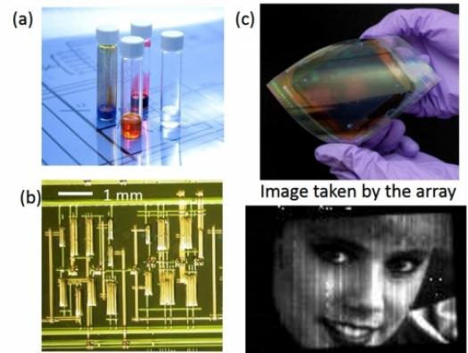
As a demonstration of this technology, Ng and her colleagues built a digital X-ray sensor. Using printing techniques, the researchers fabricated flexible X-ray imager arrays on plastic films that are much more portable than the behemoths at your dentist's office. Such a device could be used by doctors in the field, serve as small security scanners or even help soldiers identify bombs in battle.
The researchers are also working on printing an actuator, a simple mechanical device. Unlike typical silicon actuators, the printable actuator is based on solution-processed organic materials and behaves like "artificial muscles." While they haven't developed specific applications for such an actuator, Ng said, it could be used in conjunction with photo imagers to make adaptive optical parts that tune focal distance, or to make moving mirrors that redirect light beams.
This printing technique won't work for producing the high-end silicon chips in your computers and phones, Ng said. Instead, "we're going for more high-volume, simple but useful systems." In the future, for example, you might be able to print sensors onto clothing or some other device attached to the skin to monitor vital signs -- and alert a doctor in case of emergency. Some researchers have also been printing devices to make flexible solar cells; imagine wearing a jacket that doubles as a solar panel. Another possibility, Ng said, is to print flexible antennae for wireless communication.
Authors of this presentation are affiliated with Palo Alto Research Center (PARC), a Xerox Company, in California; Simon Fraser University in Canada; and Soonchunhyang University in South Korea.


