
New technique allows low-cost creation of 3-D nanostructures
Researchers from North Carolina State University have developed a new lithography technique that uses nanoscale spheres to create three-dimensional (3-D) structures with biomedical, electronic and photonic applications. The new technique is significantly less expensive than conventional methods and does not rely on stacking two-dimensional (2-D) patterns to create 3-D structures.
"Our approach reduces the cost of nanolithography to the point where it could be done in your garage," says Dr. Chih-Hao Chang, an assistant professor of mechanical and aerospace engineering at NC State and senior author of a paper on the work.
Most conventional lithography uses a variety of techniques to focus light on a photosensitive film to create 2-D patterns. These techniques rely on specialized lenses, electron beams or lasers -- all of which are extremely expensive. Other conventional techniques use mechanical probes, which are also costly. To create 3-D structures, the 2-D patterns are essentially printed on top of each other.
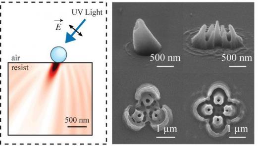
The NC State researchers took a different approach, placing nanoscale polystyrene spheres on the surface of the photosensitive film.
The nanospheres are transparent, but bend and scatter the light that passes through them in predictable ways according to the angle that the light takes when it hits the nanosphere. The researchers control the nanolithography by altering the size of the nanosphere, the duration of light exposures, and the angle, wavelength and polarization of light. The researchers can also use one beam of light, or multiple beams of light, allowing them to create a wide variety of nanostructure designs.
"We are using the nanosphere to shape the pattern of light, which gives us the ability to shape the resulting nanostructure in three dimensions without using the expensive equipment required by conventional techniques," Chang says. "And it allows us to create 3-D structures all at once, without having to make layer after layer of 2-D patterns."
The researchers have also shown that they can get the nanospheres to self-assemble in a regularly-spaced array, which in turn can be used to create a uniform pattern of 3-D nanostructures.
"This could be used to create an array of nanoneedles for use in drug delivery or other applications," says Xu Zhang, a Ph.D. student in Chang's lab and lead author of the paper.
The new technique could also be used to create nanoscale "inkjet printers" for printing electronics or biological cells, or to create antennas or photonic components.
"For this work, we focused on creating nanostructures using photosensitive polymers, which are commonly used in lithography," Zhang says. "But the technique could also be used to create templates for 3-D structures using other materials."
The researchers are currently looking at several additional ways to manipulate the technique to control the shape of resulting structures.
"We're exploring the use of nanosphere materials other than polystyrene, as well as nanoparticle shapes other than spheres," Chang says. "And ultimately we want to look at ways of controlling the placement of particles on the photosensitive film in patterns other than uniform arrays."


