
Purdue University achieves semiconductor milestone with germanium
A laboratory at Purdue University provided a critical part of the world's first transistor in 1947 "“ the purified germanium semiconductor "“ and now researchers here are on the forefront of a new germanium milestone.
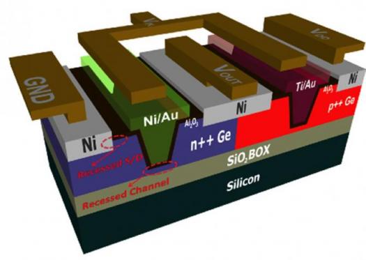
The team has created the first modern germanium circuit "“ a complementary metal"“oxide"“semiconductor (CMOS) device "“ using germanium as the semiconductor instead of silicon.
"Bell Labs created the first transistor, but the semiconductor crystal made of purified germanium was provided by Purdue physicists," said Peide "Peter" Ye, a Purdue professor of electrical and computer engineering.
Germanium was superseded by silicon as the semiconductor of choice for commercial CMOS technology. However, the industry will soon reach the limit as to how small silicon transistors can be made, threatening future advances. Germanium is one material being considered to replace silicon because it could enable the industry to make smaller transistors and more compact integrated circuits, Ye said.
Compared to silicon, germanium also is said to have a "higher mobility" for electrons and electron "holes," a trait that makes for ultra-fast circuits.
In new findings, Purdue researchers show how to use germanium to produce two types of transistors needed for CMOS electronic devices. The material had previously been limited to "P-type" transistors. The findings show how to use the material also to make "N-type" transistors. Because both types of transistors are needed for CMOS circuits, the findings point to possible applications for germanium in computers and electronics, he said.
Findings will be detailed in two papers being presented during the 2014 IEEE International Electron Devices Meeting on Dec. 15-17 in San Francisco. One paper was authored by Ye and graduate students Heng Wu, Nathan Conrad and Wei Luo, the same authors of the second paper together with graduate students Mengwei Si, Jingyun Zhang and Hong Zhou.
The material has properties that make it difficult to create an N-type contact with low electrical resistance for good current flow. However, the germanium is doped, or impregnated with impurities that alter its properties. The areas containing the most impurities have the lowest resistance. The researchers showed how to etch away the top layer of germanium, exposing the most heavily doped portion, which provides a good contact.
The etching creates recessed channels, which serve as gates needed for CMOS transistors to switch on and off. Findings show the fundamental part of the circuit, called the inverter, is the best-performing non-silicon inverter demonstrated so far, Ye said.
The research, based at the Birck Nanotechnology Center in Purdue's Discovery Park, are funded in part by the Semiconductor Research Corp.


