Cool Silicon sets International Standards

Research results from a collaborative project between NaMLab (TU Dresden), the Fraunhofer Institute for Photonic Micro Systems (IPMS) and GLOBALFOUNDRIES are being included in the current version of "˜The International Technology Roadmap for Semiconductors', the technical guide for the semiconductor branch. The development project was achieved at "˜Cool Memory', a sub-project of Cool Silicon, the leading edge cluster for energy efficient micro-and-nanoelectronics funded by the Federal Ministry for Education and Research.
Based on doped Hafniumoxide, the team has developed a cost-effective, energy-efficient ferroelectric non-volatile memory chip that requires low write voltage, can be produced at small structural width and whose production can easily be integrated in common semiconductor manufacturing processes.
Dr. Thomas Mikolajiick, Professor for Nanoelectronic Materials and Director of the NaMLab at TU Dresden, as well as the coordinator for Cool Silicon says the project's inclusion in the International Technology Roadmap is a confirmation of the success of the team's innovative work.
"For an innovation made in Dresden to become part of the International Technology Roadmap guidelines, is certainly not commonplace," Dr. Mikolajiick says. "We are very proud of this accomplishment because the roadmap is followed closely by members of the international semiconductor industry."
The new technology is a result of the Cool Silicon sub-project called "˜Cool Memory', developed by participating partners searching for innovative ways to manufacture non-volatile memory.
"Typical technologies currently used for non-volatile memory are based on the principle of charge-storage," Mikolajick says. "This has several disadvantages. Writing, for instance, requires high voltage and is very energy intensive. Due to the high voltage, certain circuit parts for controlling memory cannot be reduced to desired sizes, which renders such memory inefficient for small and medium storage densities."
Therefore, the Dresden scientists rely on a different technology. They store data in ferroelectrics, a material that can be brought into two different polarization states by means of electric charge and switching requires very little energy.
"This is nothing fundamentally new," Mikolajick says. "The approach has been used since the 1950s. Up until now, the problem has been that manufacturing required complicated materials like lead zirconium titanate (PZT). For chip manufacture, this has posed two challenges: manufacturing requires measures that are very intrusive to typical semiconductor processes; and scaling below 120 nanometers is impossible."
In order to realize the dream of a scalable and cost-effective ferroelectric memory chip, Cool Memory relies on hafnium oxide, a material which is already standard in the 28-nanometer production in the factories of project partner GLOBALFOUNDRIES where it is used as a high-k-material (high-k-dielectric). Using doping, the Dresden scientists were able to turn hafnium oxide ferroelectric and they achieved it using conventional manufacturing processes.
Now, the Saxon Leading Edge Cluster is able to produce non-volatile memory chips that enable more energy efficient writing and require lower voltage than chips currently available. They are also much easier to integrate into CMOS (Complementary Metal-Oxide-Semiconductor) processes than conventional ferroelectrics. (CMOS is a technology for constructing integrated circuits.)
Doped hafnium oxide makes manufacturing at very small structural width possible.
"The fact that this innovation is being included into the ITRS shows us how large the interest is especially from the industry," Mikolajick says. "We are delighted that the work of the Leading Edge Cluster Cool Silicon has found such great international resonance."
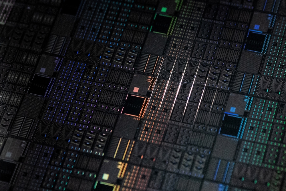
The first functioning samples of this new version of memory storage-cells scaled to a structural width of 28 nanometers - have already been produced at the Frauhofer IPMS Center for Nanoelectronic Technologies in collaboration with GLOBALFOUNDRIES. According to Fraunhofer project manager Johannes Mueller, the results are very promising:
"In the near future we hope to be able to equip microchips for future generations of more energy efficient smart phones, for instance, with memory developed and produced in Dresden," Mueller says. "This would be a huge success for Dresden scientists and for Dresden as an industry location."


