ZEISS 3D X-ray Imaging Solutions for Advanced Packaging Failure Analysis
ZEISS has unveiled a new suite of high-resolution 3D X-ray imaging solutions for failure analysis (FA) of advanced semiconductor packages, including 2.5/3D and fan-out wafer-level packages. The new ZEISS systems include the Xradia 600-series Versa and Xradia 800 Ultra X-ray microscopes (XRM) for submicron and nanoscale package FA, respectively, as well as the new Xradia Context microCT. With the addition of these new systems to its existing family of products, ZEISS now provides the broadest portfolio of 3D X-ray imaging technologies serving the semiconductor industry.
"Throughout its 170-year history, ZEISS has pushed the frontiers of scientific research and advanced the start-of-the-art in imaging technologies to enable new industrial applications and technological innovations," stated Dr. Raj Jammy, president, ZEISS Process Control Solutions (PCS) and Carl Zeiss SMT, Inc. "Now more than ever in the semiconductor industry, where package as well as device features are shrinking in all three dimensions, new imaging solutions are needed to quickly isolate failures in order to enable higher package yields. We are extremely pleased to announce this trio of new 3D X-ray imaging solutions for advanced semiconductor packaging, which provides our customers with a powerful high-resolution toolset to improve their failure analysis success rates."
Advanced Packaging Requires New Defect Detection and Failure Analysis Methods
As the semiconductor industry approaches the limits of CMOS scaling, semiconductor packaging needs to help bridge the performance gap. To continue producing ever-smaller and faster devices with lower power requirements, the semiconductor industry is turning to package innovation through 3D stacking of chips and other novel packaging formats. This drives increasingly complex package architectures and new manufacturing challenges, along with increased risk of package failures. Furthermore, since the physical location of failures is often buried within these complex 3D structures, conventional methods for visualizing failure locations are becoming less effective. New techniques are required to efficiently isolate and determine the root cause of failures in these advanced packages.
To address these needs, ZEISS has developed a new suite of 3D X-ray imaging solutions that provides submicron and nanoscale 3D images of features and defects buried within intact structures in advanced package 3D architectures. This is enabled by rotating a sample and capturing a series of 2D X-ray images from different perspectives, followed by reconstruction of 3D volumes using sophisticated mathematical models and algorithms. An unlimited number of virtual cross-sections of the 3D volume may be viewed from any angle – providing valuable insight of failure locations prior to physical failure analysis (PFA). The combination of submicron and nanoscale XRM solutions from ZEISS provides a unique FA workflow that can significantly enhance FA success rates. ZEISS's new Xradia Context microCT offers high contrast and resolution in a large field of view, using projection-based geometric magnification, and is fully upgradable to Xradia Versa.
New Imaging Solutions in Detail
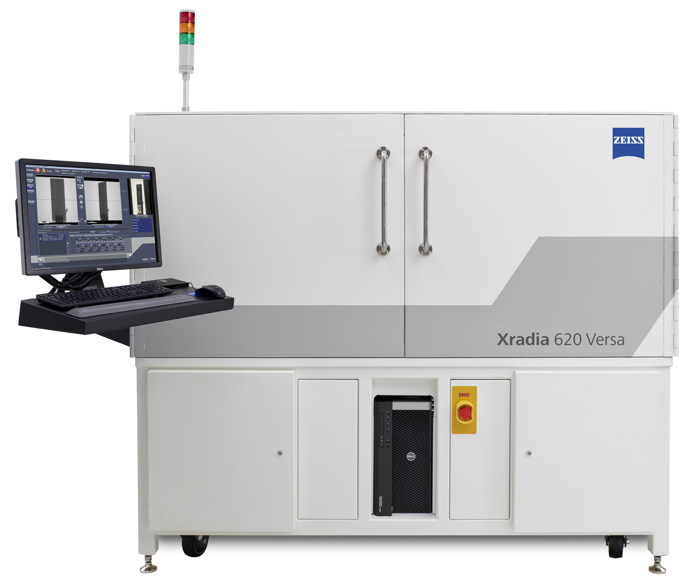
Xradia 600-series Versa is the next generation of 3D XRM for non-destructive imaging of localized defects within intact advanced semiconductor packages. It excels in structural and FA applications for process development, yield improvement and construction analysis. Based on the award-winning Versa platform with Resolution at a Distance (RaaD) capability, Xradia 600-series Versa offers unsurpassed performance for high-resolution imaging of larger samples at long working distances to determine root causes of defects and failures in packages, circuit boards and 300 mm wafers. It can easily visualize defects associated with package-level failures, such as cracks in bumps or microbumps, solder wetting problems or through silicon via (TSV) voids. The 3D visualization of defects prior to PFA reduces artifacts and guides cross-section orientations, leading to improved FA success rates. Features include:
Xradia 800 Ultra brings 3D XRM to the nanoscale realm, producing images of buried features with nanoscale spatial resolution while preserving the volume integrity of the region of interest. Applications include process analysis, construction analysis and defect analysis of ultra-fine-pitch flip chip and bump connections – enabling process improvement for ultra-fine-pitch package and back-end-of-line (BEOL) interconnects. Xradia 800 Ultra enables visualization of the texture and volume of solder consumed by intermetallic compounds in fine-pitch copper pillar microbumps. Defect sites are preserved during imaging, enabling targeted follow-up analysis by a variety of techniques. The construction quality of blind assemblies, such as wafer-to-wafer bonded interconnect and direct hybrid bonding, can be characterized in 3D. Features include:
Xradia Context microCT is a new submicron-resolution 3D X-ray microCT system based on the Versa platform. It is designed for high-resolution imaging of packages at short working distances with high throughput.