Deca Announces Chiplet Advanced Packaging Partnership with ADTEC
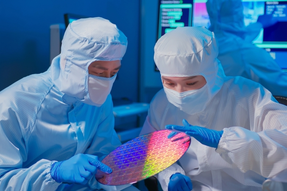
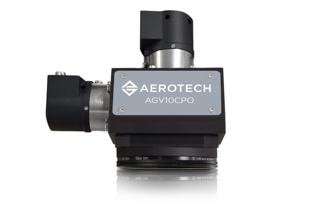
Deca, a provider of advanced electronic interconnect technologies, announced the signing of an agreement with ADTEC Engineering to join its new AP Live Network. The partnership allows ADTEC to embed an AP Connect module into its new 2µm Laser Direct Imaging (LDI) system to natively process unique Adaptive Patterning (AP) designs in real-time.
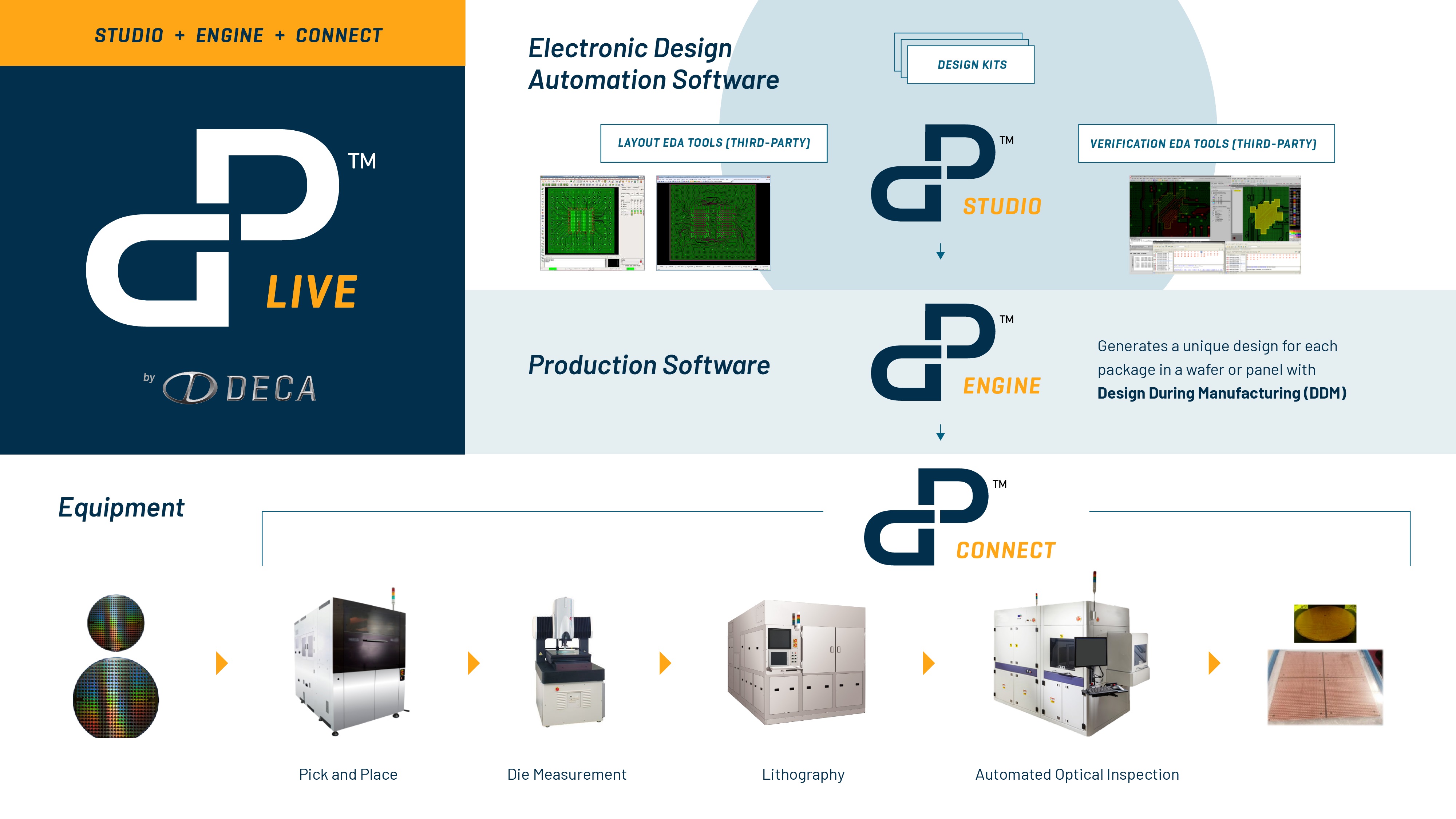
ADTEC will join Deca’s AP Live network, a growing supply chain ecosystem including original equipment manufacturers (OEMs) and electronic design automation (EDA) vendors. Deca’s AP Connect software modules embed native support for real-time AP design data into manufacturing equipment. AP Studio modules integrate the accompanying custom design flows with leading EDA systems for layout and verification.
“AP Live provides a comprehensive new capability to the backbone of the advanced packaging process, allowing OEMs like ADTEC to partner with Deca to integrate AP Connect functionality directly into their proven high-volume equipment,” said Tim Olson, founder and CEO of Deca. “Deca is pleased to cooperate with ADTEC, the industry leader in high density LDI, to bring a powerful new 2µm AP technology node to the advanced packaging industry for chiplet integration.”
ADTEC is planning to launch its cutting edge 2µm LDI system ‘DE-2’ in the spring of 2021 for advanced packaging processes, including those used in fan-out technology. Through native integration with Adaptive Patterning™, the DE-2 will provide additional essential value to customers who require fine patterning processes that deliver the highest yield.
“I am pleased that ADTEC will cooperate with Deca,” said Keizo Tokuhiro, chairman of ADTEC. “I strongly hope that the collaboration of both companies will expedite technological progress in the industry and open up a bright future.”
About Adaptive Patterning
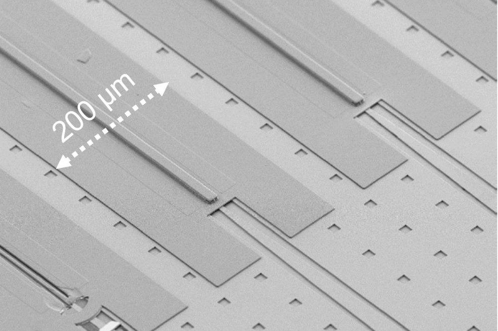
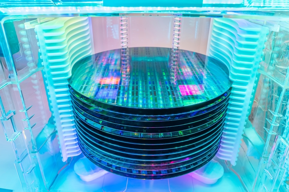
Deca’s groundbreaking Adaptive Patterning technology liberates designers and manufacturers from the constraints of fixed photomasks, allowing the production flow to account for natural variation without costly processes or design limitations. In contrast to previous techniques, AP customizes each lithographic layer on a device-by-device basis in real time as product moves through the manufacturing process, to ensure the highest possible yield and the highest performance design rules with large via contacts on ultra-fine interconnect pitch.