Loading...
News Article

PulseForge and ERS electronic collaborate

News

PulseForge, Inc. and ERS electronic GmbH have announced a strategic alliance to bring a fully-automated photonic debonding solution to the semiconductor industry.

This collaboration brings together the industry leader in thermal management solutions for semiconductor manufacturing, ERS electronic, and an industry innovator in applied thermal energy, PulseForge, Inc. ERS electronic will incorporate PulseForge’s patented Photonic Debonding process, thereby expanding their existing portfolio of thermal debond machines, which have already processed more than 2 billion IC.

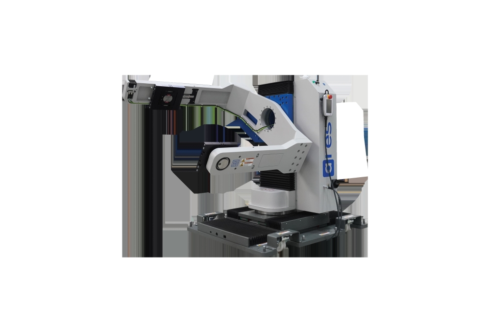
The ERS fully-automated photonic debonding solution will be ideal for the fan-out wafer-level packaging industry, combining the process and economic benefits of photonic debonding with ERS’s automation capabilities and patented AirCushion transport technology for contactless handling. Together, this will allow for streamlined operations and increased output, while maintaining the highest standards of quality. In addition, this collaboration aims to offer a fully automated debonding solution on both wafer and panel-level to address the various format requirements of the advanced packaging industry. The integration of PulseForge’s patented Photonic Debonding process will significantly reduce the total cost of ownership for debonding customers versus traditional debonding methods providing a clean and cost-effective debonding solution.

“We are excited to bring fully-automated systems to our customers for high-volume manufacturing environments by partnering with ERS electronic.” said Jonathan Gibson, CEO of PulseForge, Inc. “This partnership will provide customers with significantly lower costs for debonding processing.”

“We are thrilled to partner with the PulseForge team and combine our respective strengths to bring large-scale photonic debonding to Advanced Packaging,” says Laurent Giai-Miniet, CEO of ERS electronic. “Our 15 years of customer experience in high-volume thermal debonding will allow us to deliver a reliable, cost-effective, and high-yield system to the semiconductor manufacturing industry.”

Silicon photonics: accelerating growth in the race for high-speed optical interconnects
CCD-in-CMOS technology enables ultra-fast burst mode imaging
2025 6G A look forward
Critical Manufacturing climbs Deloitte’s Technology Fast 50
Semiconductors: The most important thing you probably know the least about
Imec and partners unveil SWIR sensor with lead-free quantum dot photodiodes
Lattice introduces small and mid-range FPGA offerings
SEMI and SMT inspection solutions at NEPCON Japan 2025
Nordic Semiconductor and Kigen demonstrate Remote SIM Provisioning for Massive IoT
Spirent collaborates with Siemens
Quobly forges strategic collaboration with STMicroelectronics
New standards in pressure measurement systems for the semiconductor industry
IBM delivers optics breakthrough
Semiconductor equipment sales to reach $139 Billion in 2026
Marvell introduces 1.6 Tbps LPO Chipset
ACM research strengthens Atomic Layer Deposition portfolio
CEA-Leti demonstrates embedded FeRAM platform compatible with 22nm FD-SOI node
Lattice introduces small and mid-range FPGA offerings
Solace unlocks full potential of event-driven integration
Advantest to showcase latest test solutions at SEMICON Japan 2024
CEA-Leti device integrates light sensing and modulation
Nordic launches Thingy:91 X prototyping platform for cellular IoT and Wi-Fi locationing
Imec achieves seamless InP Chiplet integration on 300mm RF Silicon Interposer
High-precision SMU
Powering India’s energy future
China’s Nvidia probe puts global investors ‘on notice’
POET Technologies appoints new director
Imec demonstrates core building blocks of a scalable, CMOS-fab compatible superconducting digital technology
Imec proposes double-row CFET for the A7 technology node
ULVAC launches new deposition system
Beebolt and SEMI Announce Strategic Partnership to Drive Supplier Resilience and Agility
esmo group introduces Automated Final Test Manipulator
×
Search the news archive

To close this popup you can press escape or click the close icon.
Logo
x
Logo
×
Register - Step 1

You may choose to subscribe to the Silicon Semiconductor Magazine, the Silicon Semiconductor Newsletter, or both. You may also request additional information if required, before submitting your application.


Please subscribe me to:


You chose the industry type of "Other"

Please enter the industry that you work in: