IBM delivers optics breakthrough
New co-packaged optics innovation could replace electrical interconnects in data centers to offer significant improvements in speed and energy efficiency for AI and other computing applications.
IBM has unveiled breakthrough research in optics technology that could dramatically improve how data centers train and run generative AI models. Researchers have pioneered a new process for co-packaged optics (CPO), the next generation of optics technology, to enable connectivity within data centers at the speed of light through optics to complement existing short reach electrical wires. By designing and assembling the first publicly announced successful polymer optical waveguide (PWG) to power this technology, IBM researchers have shown how CPO will redefine the way the computing industry transmits high-bandwidth data between chips, circuit boards, and servers.
Today, fiber optic technology carries data at high speeds across long distances, managing nearly all the world's commerce and communications traffic with light instead of electricity. Although data centers use fiber optics for their external communications networks, racks in data centers still predominantly run communications on copper-based electrical wires. These wires connect GPU accelerators that may spend more than half of their time idle, waiting for data from other devices in a large, distributed training process which can incur significant expense and energy.
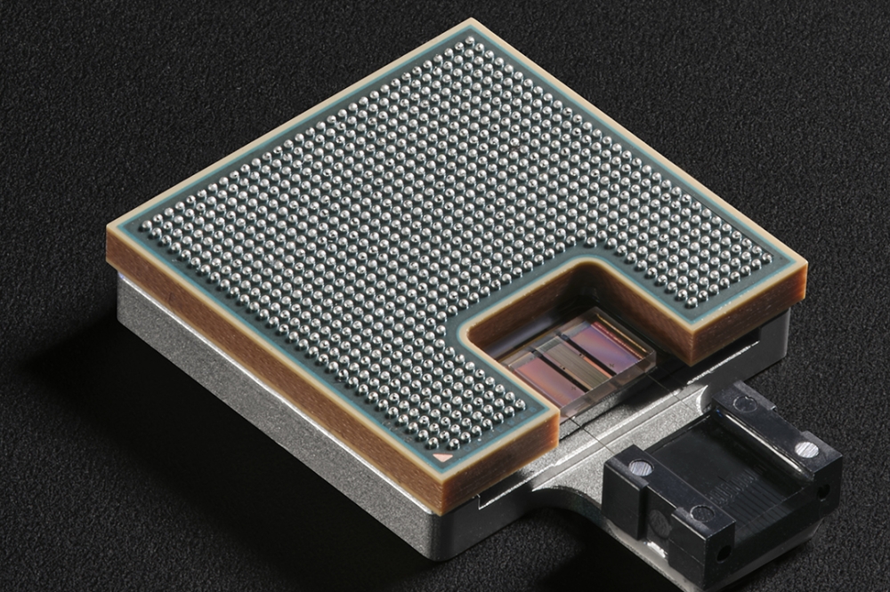
IBM researchers have demonstrated a way to bring optics’ speed and capacity inside data centers. In a technical paper, IBM introduces a new CPO prototype module that can enable high-speed optical connectivity. This technology could significantly increase the bandwidth of data center communications, minimizing GPU downtime while drastically accelerating AI processing. This research innovation, as described, would enable:
Lower costs for scaling generative AI through a more than 5x power reduction in energy consumption compared to mid-range electrical interconnects , while extending the length of data center interconnect cables from one to hundreds of meters.
Faster AI model training, enabling developers to train a Large Language Model (LLM) up to five times faster with CPO than with conventional electrical wiring. CPO could reduce the time it takes to train a standard LLM from three months to three weeks, with performance gains increasing by using larger models and more GPUs.
Dramatically increased energy efficiency for data centers, saving the energy equivalent of 5,000 U.S. homes’ annual power consumption per AI model trained.
“As generative AI demands more energy and processing power, the data center must evolve – and co-packaged optics can make these data centers future-proof,” said Dario Gil, SVP and Director of Research at IBM. “With this breakthrough, tomorrow’s chips will communicate much like how fiber optics cables carry data in and out of data centers, ushering in a new era of faster, more sustainable communications that can handle the AI workloads of the future.”
Eighty times faster bandwidth than today’s chip-to-chip communication
In recent years, advances in chip technology have densely packed transistors onto a chip; IBM’s 2 nanometer node chip technology can contain more than 50 billion transistors. CPO technology aims to scale the interconnection density between accelerators by enabling chipmakers to add optical pathways connecting chips on an electronic module beyond the limits of today’s electrical pathways. IBM’s paper outlines how these new high bandwidth density optical structures, coupled with transmitting multiple wavelengths per optical channel, have the potential to boost bandwidth between chips as much as 80 times compared to electrical connections.
IBM’s innovation, as described, would enable chipmakers to add six times as many optical fibers at the edge of a silicon photonics chip, called “beachfront density,” compared to the current state-of-the-art CPO technology. Each fiber, about three times the width of a human hair, could span centimeters to hundreds of meters in length and transmit terabits of data per second. The IBM team assembled a high-density PWG at 50 micrometer pitch optical channels, adiabatically coupled to silicon photonics waveguides, using standard assembly packaging processes.
The paper additionally indicates that these CPO modules with PWG at 50 micrometer pitch are the first to pass all stress tests required for manufacturing. Components are subjected to high-humidity environments and temperatures ranging from -40°C to 125°C, as well as mechanical durability testing to confirm that optical interconnects can bend without breaking or losing data. Moreover, researchers have demonstrated PWG technology to an 18-micrometer pitch. Stacking four PWGs would allow for up to 128 channels for connectivity at that pitch.
IBM's continued leadership in semiconductor R&D
CPO technology enables a new pathway to meet AI’s increasing performance demands, with the potential to replace off-module communications from electrical to optical. It continues IBM’s history of leadership in semiconductor innovation, which also includes the first 2 nm node chip technology, the first implementation of 7 nm and 5 nm process technologies, Nanosheet transistors, vertical transistors (VTFET), single cell DRAM, and chemically amplified photoresists.
Researchers completed design, modeling, and simulation work for CPO in Albany, New York, which the U.S. Department of Commerce recently selected as the home of America’s first National Semiconductor Technology Center (NSTC), the NSTC EUV Accelerator. Researchers assembled prototypes and tested modules at IBM’s facility in Bromont, Quebec, one of North America’s largest chip assembly and test sites. Part of the Northeast Semiconductor Corridor between the United States and Canada, IBM’s Bromont fab has led the world in chip packaging for decades.


