CEA-Leti demonstrates embedded FeRAM platform compatible with 22nm FD-SOI node
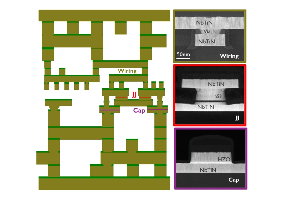
CEA-Leti research engineers have demonstrated for the first time a scalable hafnia-zirconia-based ferroelectric capacitor platform integrated into the back-end-of-line (BEOL) at the 22nm FD-SOI technology node.
This breakthrough, reported today at the IEDM 2024 conference, represents a major advance in ferroelectric memory technology, significantly advancing scalability for embedded applications and positioning ferroelectric RAM (FeRAM) as a competitive memory solution for advanced nodes.
Current embedded FeRAM products use perovskite materials, like PZT, which are not CMOS compatible and cannot scale beyond the 130nm node technology. The discovery of ferroelectricity in HfO2-based thin films, which are CMOS compatible and scalable, opens new possibilities for embedded FeRAM, but previous R&D developments were reported at the 130nm node. By pushing Hf0.5Zr0.5O2 (HZO) FeRAM technology to the 22nm FD-SOI node, this demonstration opens the door for faster, more energy-efficient, and cost-effective memory solutions in embedded systems such as IoT, mobile devices, and edge computing.
The results were presented in the IEDM paper, “Hf0.5Zr0.5O2 FeRAM Scalability Demonstration at 22nm FD-SOI Node for Embedded Applications”.
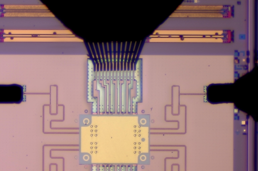
“FD-SOI technology is well-known for its low-power capability and makes it a very good fit with FeRAM, which is intrinsically the most energy efficient memory technology at bitcell level,” explained Simon Martin and Laurent Grenouillet, two main contributors to the paper. “Scaling down to 22nm required fabricating functional 2D ferroelectric capacitors down to 0.0028µm², as well as 3D ferroelectric capacitors, while keeping a relatively low thermal budget for HZO film crystallization.”
“CEA-Leti is a global leader in HfO2-based ferroelectric, thin-film research since 2018 and its continuing work is this field, including these recent results, show that the promises of this technology are becoming real,” they said.
The institute will accelerate R&D on HZO FeRAM and plans to demonstrate embedded Mbit memory arrays smaller than static random access memory (SRAM). These operate at voltages around 1V and with high access rates for ultralow-power applications requiring non-volatility. It also will work to improve HZO FeRAM reliability and explore a technology transfer to foundries.


