CEA-Leti device integrates light sensing and modulation
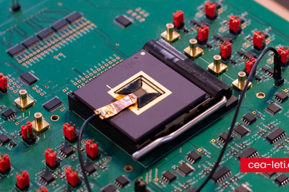
CEA-Leti researchers have developed the first-reported device able to sense light and modulate it accordingly in a single device, using a liquid crystal cell and a CMOS image sensor.
The compact system provides intrinsic optical alignment and compactness and is easy to scale-up, facilitating the use of digital optical phase conjugation (DOPC) techniques in applications such as microscopy and medical imaging.
“The main benefits of this device, which provides significant advantages compared to competing systems that require separate components, should boost its deployment in more complex and larger optical systems,” said Arnaud Verdant, CEA-Leti research engineer in mixed-signal IC design and lead-author of the paper presented at IEDM 2024.
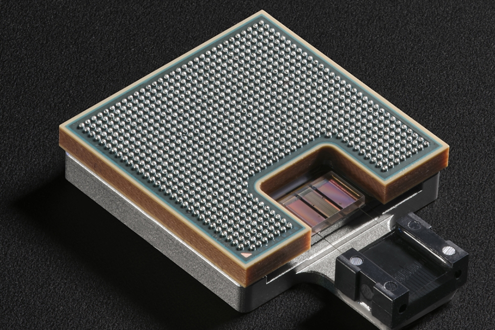
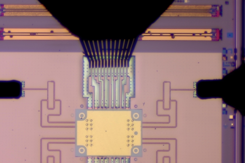
In the paper, “A 58×60 π/2-Resolved Integrated Phase Modulator And Sensor With Intra-Pixel Processing”, CEA-Leti explained that this is the first solid-state device integrating a liquid crystal-based spatial light modulator hybridized with a custom lock-in CMOS image sensor. The integrated phase modulator and sensor embeds a 58×60 pixel array, where each pixel both senses and modulates light phases.
The device leverages the key advantage of DOPC to dynamically compensate for optical wavefront distortions, which improves performance in a variety of photonic applications and corrects optical aberrations in imaging systems. By precisely controlling laser beams, it improves the resolution and penetration depth of optical imaging techniques for biomedical applications.
Standard DOPC systems rely on separated cameras and light-wavefront modulators, but their bandwidth is limited by the data processing and transfer between these devices. If the system senses and controls the light-phase modulation locally in each pixel, the bandwidth no longer depends on the number of pixels, and is only limited by the liquid crystal response time. This feature is a key advantage in fast-decorrelating, scattering media, such as living tissues.
“Scattering in biological tissues and other complex media severely limits the ability to focus light, which is a critical requirement for many photonic applications,” Verdant explained. “Wavefront shaping techniques can overcome these scattering effects and achieve focused light delivery. In the future, this will make it possible to envision applications such as photodynamic therapy, where light focusing selectively activates photosensitive drugs within tumors.
“When this technology is more mature, it also may have diverse benefits across various sectors, in addition to improving biomedical imaging resolution and depth,” he said. “It could enable earlier disease detection and non-invasive therapies. In industry, it could enhance laser beam quality and efficiency.”


