+44 (0)24 7671 8970
More publications     •     Advertise with us     •     Contact us
 
Loading...
News Article

PSMC launches the 3D AI Accelator technology platform

News

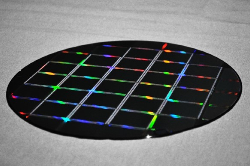
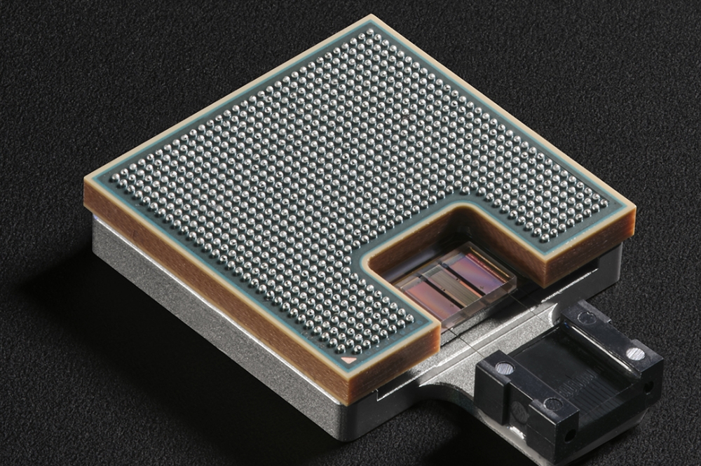
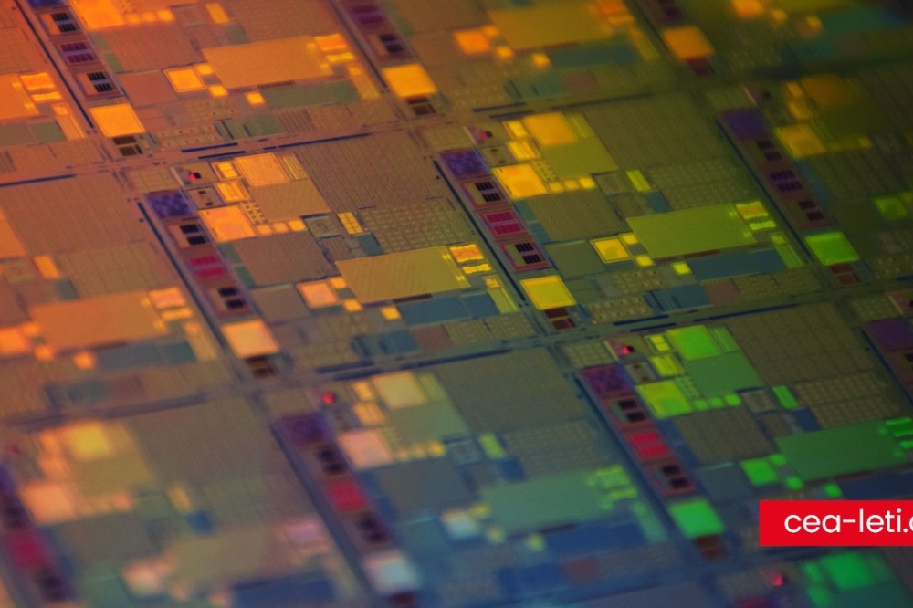
PSMC has combined the 40nm logic and 25nm DRAM processes, and used wafer stacking technology (Wafer on Wafer) to make a 3D AI accelerator.

The performance is comparable to that of commercially available 7nm systems, but the cost is said to be only a tenth of it, providing a more innovative and competitive AI chip foundry platform for the IC design industry.

In cooperation with the Industrial Technology Research Institute, Smart Memory, and Maxram, the company unveiled the AIM-200 3D AI Accelator technology platform at COMPUTEX 2023. This demonstration chip is based on two 12-inch wafers produced by PSMC's 40nm logic process and 25nm DRAM process, and is integrated by wafer stacking technology, with the data transmission between logic circuits and DRAM to be integrated in one fell swoop. The bandwidth is expanded to 1024 bits. Compared with the existing 32 or 64 bits, it can be said to break through the high memory wall (Memory Wall) that affects the system's computing performance all at once.

According to PSMC, compared with similar AI products, the AIM-200 3D AI Accelator only consumes 1/10 of the power to obtain the same CNN computing efficiency. Although the AI acceleration chip manufactured by the technology platform only uses a 40nm logic process to produce AI Engine and 25nm DRAM, its performance is comparable to similar products produced by a 7nm process, and the demonstration chip operates continuously throughout the day. However, there is still no sign of overheating due to high-speed computing, showing the 'superiority' of the ultra-high transmission bandwidth.

This breakthrough technological innovation has the potential to assist the IC design industry and reduce the cost of AI accelerators by 90%.

UK semiconductor strategy: A patent attorney’s perspective
Wafer cleaning market to reach US$ 17.2 billion
Solvay signs partnership agreement with Shengjian
ACM cleaning platform targets chiplets industry
Vietnam's thriving semiconductor industry fuels economic resilience
GSA celebrates women's innovation
The need for geofencing to help improve semiconductor IP security
All roads lead to Arizona
Time to celebrate and accelerate diversity, equity and inclusion
Cadence completes acquisition of PHY IP assets from Rambus
Wales joins the European Semiconductor Regional Alliance
Magnachip targets EV market
Greene Tweed: When it can’t fail
Advanced Packaging market Size to reach $66.9 billion by 2032
Inventec and Renesas to develop PoC for automotive gateways
Renesas commences Sequans tender offer
Tower Semiconductor and InnoLight partner
Flanders Semiconductors - a new hub in the heart of Europe
Ambiq wins Demo of the Year Award
Advanced packaging market nears US$90 billion
Intel Foundry Services and Tower Semiconductor reach US foundry agreement
MediaTek develops first chip using TSMC's 3nm Process
Advanced X-ray technology for advanced packaging
New developments in underlayers and their role in advancing EUV lithography
Advanced SAM validates integrity of electrostatic chucks
Purdue establishes permanent presence next to NSWC Crane
Bolstering semiconductor ecosystem at Texas A&M University
Semiconductor industry sees revenue increase for the first time since 2021
Bosch completes TSI Semiconductors acquisition
Semiconductor grants for undergraduate women
Sustainability rises up the automotive agenda
Lumibird completes Prima acquisitions
×
Search the news archive

To close this popup you can press escape or click the close icon.
Logo
×
Logo
×
Register - Step 1

You may choose to subscribe to the Silicon Semiconductor Magazine, the Silicon Semiconductor Newsletter, or both. You may also request additional information if required, before submitting your application.


Please subscribe me to:


You chose the industry type of "Other"

Please enter the industry that you work in: