
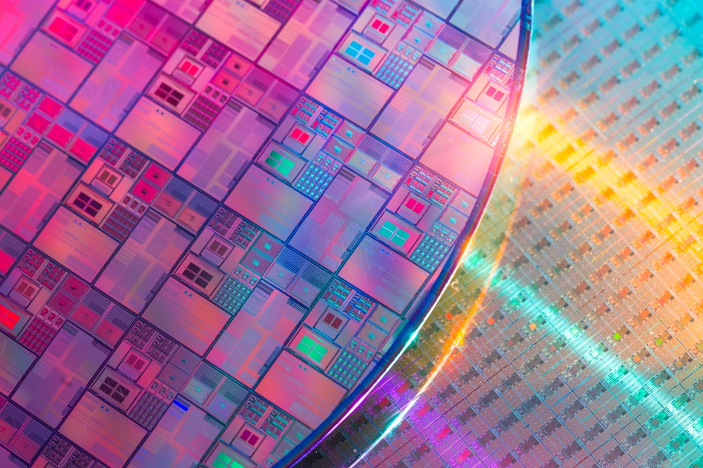
Intel implements backside power delivery in silicon
Product-like test chip shows PowerVia’s ability to deliver over 90% cell utilization, solve growing interconnect bottlenecks and bring competitive advantages to customers – including foundry.
Intel says that it is the first in the industry to implement backside power delivery on a product-like test chip, achieving the performance needed to propel the world into the next era of computing. PowerVia, which will be introduced on the Intel 20A process node in the first half of 2024, is Intel’s industry-leading backside power delivery solution. It solves the growing issue of interconnect bottlenecks in area scaling by moving power routing to the backside of a wafer.
Ben Sell, Intel Vice President of Technology Development comments: “PowerVia is a major milestone in our aggressive ‘five nodes in four years’ strategy and on our path to achieving a trillion transistors in a package in 2030. Using a trial process node and subsequent test chip enabled us to de-risk backside power for our leading process nodes, placing Intel a node ahead of competitors in bringing backside power delivery to market.”
Intel decoupled development of PowerVia from transistor development to ensure its readiness for silicon implementation based on Intel 20A and Intel 18A process nodes. PowerVia was tested on its own internal test node to debug and ensure good functionality of the technology before its integration with RibbonFET in Intel 20A. After fabrication and testing on a silicon test chip, PowerVia was confirmed to bring a remarkably efficient use of chip resources with greater than 90% cell utilization and major transistor scaling, enabling chip designers to achieve performance and efficiency gains in their products.
Intel will present these findings at the VLSI Symposium on June 11-16 in Kyoto, Japan.
Intel believes that PowerVia is well ahead of competitors’ backside power solutions, giving chip designers – including Intel Foundry Services (IFS) customers – a faster path to valuable energy and performance gains in their products. Intel has a long track record of introducing the industry’s most critical new technologies, such as strained silicon, Hi-K metal gate and FinFET, to propel Moore’s Law forward. With PowerVia and RibbonFET gate-all-around technology coming in 2024, Intel continues to lead the industry in chip design and process innovations.
Intel says that PowerVia is the first to solve the growing interconnect bottleneck issue for chip designers. Surging use cases, including artificial intelligence and graphics, require smaller, denser and more powerful transistors to meet ever-growing computing demands. Today and for the past many decades, power and signal lines within a transistor’s architecture have competed for the same resources. By separating the two, chips can increase performance and energy-efficiency, and deliver better results for customers. Backside power delivery is vital to transistor scaling, enabling chip designers to increase transistor density without sacrificing resources to deliver more power and performance than ever.
Intel 20A and Intel 18A will introduce both PowerVia backside power technology and RibbonFET gate-all-around technology. As a completely new way of delivering power to the transistors, backside power implementation raised new challenges for thermals and debugging designs.
By decoupling development of PowerVia from RibbonFET, Intel could work through those challenges quickly to ensure readiness for implementation in silicon based on Intel’s 20A and 18A process nodes. Intel engineers developed mitigation techniques to prevent the thermals from becoming an issue. The debug community also developed new techniques to ensure the new design structure could be appropriately de-bugged. As a result, the test implementation delivered solid yield and reliability metrics while demonstrating the intrinsic value proposition of the technology well before it joins new RibbonFET architecture.
The test also leveraged design rules enabled by EUV (extreme ultraviolet) lithography, which produced results including standard cell utilization of more than 90% over large areas of the die, enabling greater cell density which can be expected to lower costs. The test also showed more than 30% platform voltage droop improvement and 6% frequency benefit. Intel also achieved thermal characteristics in the PowerVia test chip in line with higher power densities expected from logic scaling.
In a third paper to be presented during VLSI, Intel technologist Mauro Kobrinsky will explain the research into more advanced methods to deploy PowerVia such as enabling both signaling and power delivery on either the front or the back side of the wafer. Bringing PowerVia to customers ahead of the industry and continuing to innovate into the future is in keeping with Intel’s long history of being first to bring new semiconductor innovations to market while constantly innovating.


