Asia takes center stage

Nanometer chips redefining semiconductor industry landscape, says GlobalData.
Nanometer chips, particularly those under 10nm, are revolutionizing the semiconductor industry with their superior performance, energy efficiency, and transistor density. These chips underpin a wide range of applications, from consumer electronics to advanced AI and machine learning systems. As the semiconductor landscape continues to evolve, there is a shift in the industry's center of gravity towards Asia, observes GlobalData, a leading data and analytics company.
Kiran Raj, Practice Head of Disruptive Tech at GlobalData, comments: “The nanometer chip revolution is here to rewrite the rules of technology. Unleashing a power surge in the AI realm, 5nm chips, for instance, are redefining speed and efficiency across industries. They are turbocharging generative AI, making edge computing nimbler, fueling smarter consumer devices, driving autonomous vehicles into the future besides influencing healthcare and quantum computing.”
An analysis of GlobalData’s Disruptor Intelligence Center emphasizes game-changing developments and plans of TSMC, Intel, Samsung, and IBM in nanometer chip technology.
TSMC, the world’s largest semiconductor foundry, has unveiled advancements in 2nm technology and new additions to its 3nm family, including N3P for improved power, performance, and density, N3X for high-performance computing applications, and N3AE for early automotive applications. Its 2nm technology, which utilizes nanosheet transistors, is slated for production in 2025. Concurrently, TSMC is pioneering N4PRF, claimed to be the industry's most advanced CMOS radio frequency (RF) technology for digital-intensive RF applications.
Samsung aims to mass-produce 2nm chips by 2025 and 1.4nm chips by 2027, leveraging its success with 3nm technology ahead of TSMC. It is also developing 2.5D/3D packaging technology, aiming to launch 3D packaging X-Cube in 2024 and a bump-less X-Cube in 2026. To support these, Samsung plans to triple its sub-10nm chip production capacity by 2027, which includes a new manufacturing line in Texas.
Intel’s 4 process, equivalent to 7nm, is production-ready, while Intel 3, analogous to 5nm, is anticipated for high-volume manufacturing in late 2023. In the same timeline, the company's Meteor Lake products, using Intel 4 for CPU cores and TSMC's N3 or N5 node for graphics, will be released. Moreover, Intel plans to debut its 20A node (roughly 2nm) in 2024, utilizing innovative RibbonFET and PowerVia technologies, set to rival TSMC's third-gen 3nm-class processes. Lastly, Intel is preparing its 18A node, equivalent to 1.8nm, for production in the second half of 2025.
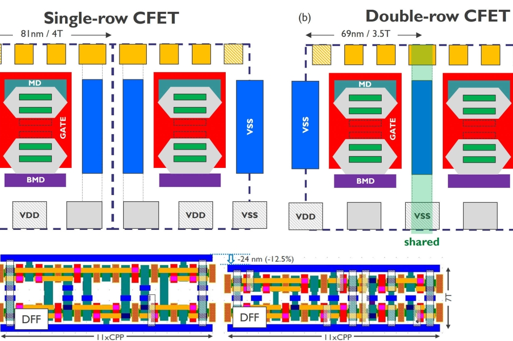
IBM's 2nm chip, employing a novel Gate-All-Around (GAA) architecture, packs 50 billion transistors into a fingernail-sized space. A significant evolution from FinFET structures, this design validates numerous minor milestones. Created at IBM's Albany facility, its production required diverse expertise, from materials to modeling.
Raj concludes: “TSMC firmly dominates the semiconductor industry, having already transitioned to groundbreaking 5nm and 4nm processes, and is poised to usher in a new era of 3nm volume production by late 2023. Nvidia’s new H100 GPU uses TSMC’s 4nm process. Meanwhile, Samsung grapples with significant production hurdles, yielding less than 50% on its 5nm node, a stark contrast to TSMC's progress. Intel trails further behind, underscoring the fiercely competitive landscape.
“Crucially, ASML, the exclusive manufacturer of EUV lithography machines essential for these advances, predominantly serves clients like TSMC and Samsung. This trend strongly suggests that the center of gravity in the semiconductor industry will continue its shift toward Asia, further strengthening its stranglehold on this crucial technology sector.”


